
User guide


Chapter 5: Functional Description—ALTMEMPHY 5–41
Using a Custom Controller
December 2010 Altera Corporation External Memory Interface Handbook Volume 3
Section II. DDR3 SDRAM Controller with ALTMEMPHY IP User Guide
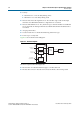
The
ctl_wlat
signal is only valid when the calibration has been successfully
completed by the ALTMEMPHY sequencer and does not change at any point during
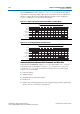
normal user mode operation. Figure 5–23 shows the operation of
ctl_wlat
port.
For a half-rate design
ctl_cs_n
is 2 bits, not 1. Also the
ctl_dqs_burst
and
ctl_wdata_valid
waveforms indicate a half-rate design. This write results in a burst
of 8 at the DDR. Where
ctl_cs_n
is driven 2'
b01
, the LSB (1) is the first value driven
out of
mem_cs_n
, and the MSB (0) follows on the next
mem_clk
. Similarly, for
ctl_dqs_burst
, the LSB is driven out of
mem_dqs
first (0), then a 1 follows on the next
clock cycle. This sequence produces the continuous DQS pulse as required. Finally,
the
ctl_addr
bus is twice
MEM_IF_ADDR_WIDTH
bits wide and so the address is
concatenated to result in an address phase two
mem_clk
cycles wide.
Partial Writes
As part of the DDR3 SDRAM memory specifications, you have the option for partial
write operations by asserting the DM pins for part of the write signal.
For designs targeting the Arria II and Stratix III devices, deassert the
ctl_wdata_valid
signal during partial writes, when the write data is invalid, to save power by not
driving the DQ outputs.
For designs targeting other devices, use only the DM pins if you require partial writes.
Assert the
ctl_dqs_burst
and
ctl_wdata_valid
signals as for full write operations, so
that the DQ and DQS pins are driven during partial writes.
The I/O difference between Stratix III devices and other devices, and the preamble
difference for DDR3 SDRAM on Arria II GX devices make it only possible to use the
ctl_dqs_burst
signal for the DQS enable in Stratix III devices.
Figure 5–23. Timing for ctl_dqs_burst, ctl_wdata_valid, Address, and Command—Half-Rate
Design
ctl_clk
ctl_addr
ctl_cs_n
ctl_dqs_burst
ctl_wdata_valid
ctl_wdata
AdAdAdAd
0101
10 1111
ctl_wlat = 2
1 2