
User guide


Chapter 5: Functional Description—ALTMEMPHY 5–39
Using a Custom Controller
December 2010 Altera Corporation External Memory Interface Handbook Volume 3
Section II. DDR3 SDRAM Controller with ALTMEMPHY IP User Guide
Calibration Process Requirements
When the global
reset_n
is released the ALTMEMPHY handles the initialization and
calibration sequence automatically. The sequencer calibrates memory interfaces by
issuing reads to multiple ranks of DDR3 SDRAM (multiple chip select). Timing
margins decrease as the number of ranks increases. It is impractical to supply one
dedicated resynchronization clock for each rank of memory, as it consumes PLL
resources for the relatively small benefit of improved timing margin. When
calibration is complete
ctl_cal_success
goes high if successful;
ctl_cal_fail
goes
high if calibration fails. Calibration can be repeated by the controller using the
soft_reset_n
signal, which when asserted puts the sequencer into a reset state and
when released the calibration process begins again.
Other Local Interface Requirements
The memory burst length for DDR3 SDRAM devices can be set at either four or eight;
but when using the Altera high-performance controller, only burst length eight is
supported. For a half-rate controller, the memory clock runs twice as fast as the clock
provided to the local interface, so data buses on the local interface are four times as
wide as the memory data bus.
Address and Command Interfacing
Address and command signals are automatically sized for
1T
operation, such that for
full-rate designs there is one input bit per pin (for example, one
cs_n
input per
chip select configured); for half-rate designs there are two. If you require a more
conservative
2T
address and command scheme, use a full-rate design and drive the
address/command inputs for two clock cycles, or in a half-rate design drive both
address/command bits for a given pin identically.
1 Although the PHY inherently supports
1T
addressing, the high-performance
controllers support only
2T
addressing, so PHY timing analysis is performed
assuming
2T
address and command signals.
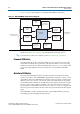
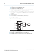
Handshake Mechanism Between Read Commands and Read Data
When performing a read, a high-performance controller with the AFI asserts
ctl_doing_read
to indicate that a read command is requested and the byte lanes that
it expects valid data to return on. ALTMEMPHY uses
ctl_doing_read
for the
following actions:
■ Control of the postamble circuit
■ Generation of
ctl_rdata_valid
■ Dynamic termination (Rt) control timing
The read latency,
ctl_rlat
, is advertised back to the controller. This signal indicates
how long it takes in
ctl_clk
clock cycles from assertion of
ctl_doing_read
to valid
read data returning on
ctl_rdata
. The
ctl_rlat
signal is only valid when calibration
has successfully completed and never changes values during normal user mode
operation.