
User guide


Chapter 5: Functional Description—ALTMEMPHY 5–37
PHY-to-Controller Interfaces
December 2010 Altera Corporation External Memory Interface Handbook Volume 3
Section II. DDR3 SDRAM Controller with ALTMEMPHY IP User Guide
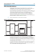
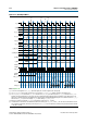
Figure 5–20. Word-Unaligned Reads
Notes to Figure 5–20:
(1) Similar to word-aligned reads,
ctl_doing_rd
is asserted one memory clock cycle before chip select (
ctl_cs_n
) is asserted, which for a
word-unaligned read is in the previous controller clock (
ctl_clk
) cycle. In this example the
ctl_doing_rd
signal is now spread over three
controller clock (
ctl_clk
) cycles, the high bits in the sequence '10','11','01','10','11','01' providing the required four memory clock cycles of
assertion for
ctl_doing_rd
for the two 4-beat reads in the full-rate memory clock domain, '011110','011110'.
(2) The return pattern of
ctl_rdata_valid
is a delayed version of
ctl_doing_rd
. Advertised read latency (
ctl_rlat
) is the number of controller
clock (
ctl_clk
) cycles delay inserted between
ctl_doing_rd
and
ctl_rdata_valid
.
(3) The read data (
ctl_rdata
) is spread over three controller clock cycles and in the pointed to vector only the upper half of the
ctl_rdata
bit vector
is valid (denoted by
ctl_rdata_valid
).
ctl_clk
ctl_rlat
ctl_ras_n
ctl_cas_n
ctl_we_n
ctl_cs_n
ctl_doing_rd
ctl_rdata_valid
ctl_rdata
ctl_ba
ctl_addr
ctl_dm
Memory
Interface
mem_clk
command
mem_cs_n
mem_dqs
mem_dq
(2)(1)
(3)
00 00 10
15
11
11 10 11 10 11
00
00 10 11 01 10 11 01 0
00
00
00
10 11 01 10 11 01 00
FFFFFFFF
FFFFFFFF
0f0e0f0e
0000000
ACT RD