
User guide


5–36 Chapter 5: Functional Description—ALTMEMPHY
PHY-to-Controller Interfaces
External Memory Interface Handbook Volume 3 December 2010 Altera Corporation
Section II. DDR3 SDRAM Controller with ALTMEMPHY IP User Guide
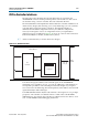
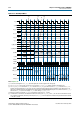
Figure 5–19 and Figure 5–20 show spaced word-unaligned writes and reads.
Figure 5–19. Word-Unaligned Writes
Notes to Figure 5–19:
(1) Alternative word-unaligned chip select (
ctl_cs_n
).
(2) As with word- aligned writes,
ctl_dqs_burst
is asserted one memory clock cycle before
ctl_wdata_valid
. You can see
ctl_dqs_burst
is
11 in the same cycle where
ctl_wdata_valid
is 10. The LSB of these two becomes the first value the signal takes in the
mem_clk
domain. You
can see that
ctl_dqs_burst
has the necessary one
mem_clk
cycle lead on
ctl_wdata_valid
.
(3) The latency between ctl_cs_n being asserted and
ctl_wdata_valid
going high is effectively
ctl_wlat
(in this example, two) controller clock
(ctl_clk) cycles. This can be thought of in terms of relative memory clock (
mem_clk
) cycles, in which case the latency is four
mem_clk
cycles.
(4) Only the upper half is valid (as the
ctl_wdata_valid
signal demonstrates, there is one
ctl_wdata_valid
bit to two 8-bit words). The write
data bits go out on the bus in order, least significant byte first. So for a continuous burst of write data on the DQ pins, the most significant half of
write data is used, which goes out on the bus last and is therefore contiguous with the following data. The converse is true for the end of the burst.
Write data is spread across three controller clock (
ctl_clk
) cycles, but still only four memory clock (
mem_clk
) cycles. However, in relative
memory clock cycles the latency is equivalent in the word-aligned and word-unaligned cases.
(5) The
0504
here is residual from the previous clock cycle. In the same way that only the upper half of the write data is used for the first beat of the
write, only the lower half of the write data is used in the last beat of the write. These upper bits can be driven to any value in this alignment.
ctl_clk
ctl_wlat
ctl_ras_n
ctl_cas_n
ctl_we_n
ctl_cs_n
ctl_dqs_burst
ctl_wdata_valid
ctl_wdata
ctl_ba
ctl_addr
Memory
Interface
mem_clk
command
mem_cs_n
mem_dqs
mem_dq
(4)(2)
(1)
(5)(3)
1010
2
01
01 00
01
01 00
11
11 10 11 10 11
00
00
00
11 01 11 01 00
00
00 10 11 01 10 11 01 00
00000000
00000000
01000000 05040302 05040706 09080706 0d0c0b0a
0d0c0f0e
0000000 0000000
020000
020008
ACTACT WR