
User guide


Chapter 5: Functional Description—ALTMEMPHY 5–31
PHY-to-Controller Interfaces
December 2010 Altera Corporation External Memory Interface Handbook Volume 3
Section II. DDR3 SDRAM Controller with ALTMEMPHY IP User Guide
PHY-to-Controller Interfaces
The following section describes the typical modules that are connected to the
ALTMEMPHY variation and the port name prefixes each module uses. This section
also describes using a custom controller. This section describes the AFI.
The AFI standardizes and simplifies the interface between controller and PHY for all
Altera memory designs, thus allowing you to easily interchange your own controller
code with Altera's high-performance controllers. The AFI PHY includes an
administration block that configures the memory for calibration and performs
necessary mode registers accesses to configure the memory as required (these
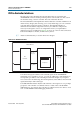
calibration processes are different). Figure 5–14 shows an overview of the connections
between the PHY, the controller, and the memory device.
1 Altera recommends that you use the AFI for new designs.
For half-rate designs, the address and command signals in the ALTMEMPHY
megafunction are asserted for one
mem_clk
cycle (1T addressing), such that there are
two input bits per address and command pin in half-rate designs. If you require a
more conservative 2T addressing, drive both input bits (of the address and command
signal) identically in half-rate designs.
For DDR3 SDRAM with the AFI, the read and write control signals are on a per-DQS
group basis. The controller can calibrate and use a subset of the available DDR3
SDRAM devices. For example, the controller can calibrate and use two devices out of
a 64- or 72-bit DIMM for better debugging mechanism.
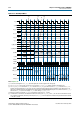
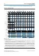
Figure 5–14. AFI PHY Connections
AFI
Controller
local_wdata
local_rdata
ctl_addr
ctl_cas_n
ctl_we_n
ctl_rdata
Admin
Sequencer
AFI PHY
mem_dqs
mem_dq
DDR3
SDRAM
Altera Device