
User guide


Chapter 5: Functional Description—ALTMEMPHY 5–29
ALTMEMPHY Signals
December 2010 Altera Corporation External Memory Interface Handbook Volume 3
Section II. DDR3 SDRAM Controller with ALTMEMPHY IP User Guide
hc_scan_enable_
access
Input 1
This signal switches the control of the levelling delay chains from the
sequencer to the
hc_scan_
signals. It should normally be tied low.
hc_scan_enable_dq Input
MEM_IF_
DWIDTH
When
hc_scan_enable_access
is asserted, this bus directly
connects to the
ena
inputs on the
IO_CONFIG
atoms for every DQ
pin. Otherwise, this input has no effect.
hc_scan_enable_dm Input
MEM_IF_D
M_
DWIDTH
When
hc_scan_enable_access
is asserted, this bus directly
connects to the
ena
inputs on the
IO_CONFIG
atoms for every DM
pin. Otherwise, this input has no effect.
hc_scan_enable_
dqs
Input
MEM_IF_D
QS_
DWIDTH
When
hc_scan_enable_access
is asserted, this bus directly
connects to the
ena
inputs on the
IO_CONFIG
atoms for every DQS
pin. Otherwise, this input has no effect.
hc_scan_enable_
dqs_config
Input
MEM_IF_D
QS_
DWIDTH
When
hc_scan_enable_access
is asserted, this bus directly
connects to the
ena
inputs on the
DQS_CONFIG
atoms for every DQS
pin. Otherwise, this input has no effect.
hc_scan_din Input
MEM_IF_D
QS_
DWIDTH
When
hc_scan_enable_access
is asserted, this bus directly
connects to the
datain
inputs on the
IO_CONFIG
and
DQS_CONFIG
atoms for every DQ, DM, and DQS pin. Otherwise, this input has no
effect.
hc_scan_update Input
MEM_IF_D
QS_
DWIDTH
When
hc_scan_enable_access
is asserted, this bus directly
connects to the
update
inputs on the
IO_CONFIG
and
DQS_CONFIG
atoms for every DQ, DM, and DQS pin. Otherwise, this input has no
effect.
hc_scan_ck Input 1
When
hc_scan_enable_access
is asserted, this bus directly
connects to the
clk
inputs on the
IO_CONFIG
and
DQS_CONFIG
atoms for every DQ, DM, and DQS pin. Otherwise, this input has no
effect.
hc_scan_dout Output
MEM_IF_
DWIDTH
When
hc_scan_enable_access
is asserted, a multiplexer connects
this bus to the relevant
dataout
outputs of the
IO_CONFIG
or
DQS_CONFIG
atoms for the signal group which is currently being
selected via the
hc_scan_enable_
signals. Otherwise, this input
has no effect.
Calibration Interface Signals—without leveling only
rsu_codvw_phase
Output —
The sequencer sweeps the phase of a resynchronization clock across
360° or 720° of a memory clock cycle. Data reads from the DIMM
are performed for each phase position, and a data valid window is
located, which is the set of resynchronization clock phase positions
where data is successfully read. The final resynchronization clock
phase is set at the center of this range: the center of the data valid
window or CODVW. This output is set to the current calculated value
for the CODVW, and represents how many phase steps were
performed by the PLL to offset the resynchronization clock from the
memory clock.
rsu_codvw_size
Output —
The final centre of data valid window size (
rsu_codvw_size
) is the
number of phases where data was successfully read in the
calculation of the resynchronization clock centre of data valid
window phase (
rsu_codvw_phase
).
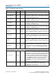
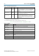
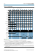
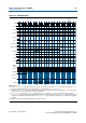
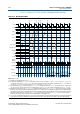
Table 5–5. Other Interface Signals (Part 3 of 4)
Signal Name Type Width Description