
User guide


Chapter 5: Functional Description—ALTMEMPHY 5–25
ALTMEMPHY Signals
December 2010 Altera Corporation External Memory Interface Handbook Volume 3
Section II. DDR3 SDRAM Controller with ALTMEMPHY IP User Guide
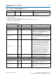
mem_err_out_n (4) Input 1
The signal sent from the DIMM to the PHY to
indicate that a parity error has occured for a
particular cycle.
Notes to Table 5–3:
(1) Connected to I/O pads.
(2) Refer to Table 5–6 for parameter description.
(3) Output is for memory device, and input path is fed back to ALTMEMPHY megafunction for VT tracking.
(4) This signal is for Registered DIMMs only.
Table 5–3. Interface to the DDR3 SDRAM Devices (Note 1)
Signal Name Type Width (2) Description
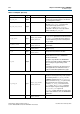
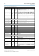
Table 5–4. AFI Signals (Part 1 of 3)
Signal Name Type Width (1) Description
Clocks and Resets
pll_ref_clk
Input 1 The reference clock input to the PHY PLL.
global_reset_n
Input 1
Active-low global reset for PLL and all logic in the
PHY. A level set reset signal, which causes a
complete reset of the whole system. The PLL may
maintain some state information.
soft_reset_n
Input 1
Edge detect reset input intended for SOPC Builder
use or to be controlled by other system reset logic.
Causes a complete reset of PHY, but not the PLL
used in the PHY.
reset_request_n
Output 1
Directly connected to the locked output of the PLL
and is intended for optional use either by automated
tools such as SOPC Builder or could be manually
ANDed with any other system-level signals and
combined with any edge detect logic as required
and then fed back to the
global_reset_n
input.
Reset request output that indicates when the PLL
outputs are not locked. Use this as a reset request
input to any system-level reset controller you may
have. This signal is always low while the PLL is
locking (but not locked), and so any reset logic
using it is advised to detect a reset request on a
falling-edge rather than by level detection.
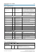
ctl_clk
Output 1
Half-rate clock supplied to controller and system
logic. The same signal as the non-AFI
phy_clk
.
ctl_reset_n
Output 1 Reset output on
ctl_clk
clock domain.
Other Signals
aux_half_rate_clk
Output 1
In half-rate designs, a copy of the
phy_clk_1x
signal that you can use in other parts of your
design, same as
phy_clk
port.
aux_full_rate_clk
Output 1
In full-rate designs, a copy of the
mem_clk_2x
signal that you can use in other parts of your
design.