
User guide


Chapter 5: Functional Description—ALTMEMPHY 5–23
ALTMEMPHY Signals
December 2010 Altera Corporation External Memory Interface Handbook Volume 3
Section II. DDR3 SDRAM Controller with ALTMEMPHY IP User Guide
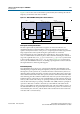
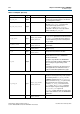
Figure 5–12 shows the reordered or the reordered-and-delayed HDR data is then
converted to DDR data within the IOE element using both the half-rate and full-rate
clocks.
The write datapath DDIO registers are clocked by the
phy_clk_1x
clock. The
write_clk_2x
signal then clocks the alignment registers.
f For more information about the I/O structure, refer to the External Memory Interface
chapter in the respective device family handbook.
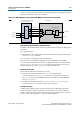
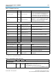
Figure 5–13 shows how the write data,
ctl_wdata
signals should be aligned from the
controller during a (half rate, normally aligned) write operation. The PHY then issues
the write data as ABCD where a is the first data to be written to the memory. (ABCD
represent two beats of data each.) The
ctl_wdata_valid
signal in Figure 5–13 shows
the output enable for the DQ and DM pins.
ALTMEMPHY Signals
This section describes the ALMEMPHY megafunction signals for DDR3 SDRAM
variants.
Table 5–3 through Table 5–5 show the signals.
Figure 5–12. DDR3 SDRAM Write Datapath in Stratix IV and Stratix III Devices
[
Data
Ordering
Data Ordering
HDR to DDR
Conversion
mem_dq
Stratix III
IOE
write_clk_2x
phy_clk_1x
ctl_wdata[4n]
phy_clk_1x
wdp_wdata3_1x
wdp_wdata2_1x
wdp_wdata1_1x
wdp_wdata0_1x
Figure 5–13. Write Data Alignment from the DDR3 SDRAM Controller
00
10
11
00
00
11
00
-- ba --dc
ctl_clk
ctl_dqs_burst
ctl_wdata_valid
ctl_wdata