
User guide


Chapter 5: Functional Description—ALTMEMPHY 5–21
Block Description
December 2010 Altera Corporation External Memory Interface Handbook Volume 3
Section II. DDR3 SDRAM Controller with ALTMEMPHY IP User Guide
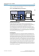
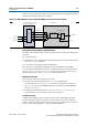
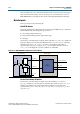
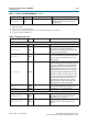
Figure 5–10 shows the order of the functions performed by the read datapath and the
frequency at which the read data is handled.
Data Capture, Resynchronization, and Demultiplexing
The IOE in Stratix III and Stratix IV devices performs the following tasks during read
operation:
■ Captures the data
■ Resynchronizes the captured data from the DQS domain to the resynchronization
clock (
resync_clk_1x
) domain
■ Converts the resynchronized data into HDR data
This operation is performed by feeding the resynchronized data into the HDR
conversion block within the IOE, which is clocked by the half-rate resynchronization
clock (
resync_clk_1x
). The
resync_clk_1x
signal is generated from the I/O clock
divider module, based on the
resync_clk_2x
signal from the PLL.
Read Data Storage Logic
The read block performs the following two tasks:
■ Transfers the captured read data (
rdata[n]_1x
) from the half-rate
resynchronization clock (
resync_clk_1x
) domain to the half-rate system clock
(
phy_clk_1x
) domain using DPRAM. Resynchronized data from the DPRAM is
shown as
ram_data_1x
.
■ Reorders the resynchronized data (
ram_rdata_1x
) into
ctl_mem_rdata
, to be
presented in the user clock domain in the same clock cycle.
Postamble Protection
A dedicated postamble register controls the gating of the shifted DQS signal that
clocks the DQ input registers at the end of a read operation. This ensures that any
glitches on the DQS input signals at the end of the read postamble time do not cause
erroneous data to be captured as a result of postamble glitches.
Figure 5–10. DDR3 SDRAM Data Capture and Read Data Mapping in Stratix IV and Stratix III Devices
Dual Port RAM
Read Datapath
Data Capture, Resynchronization,
and Data Demultiplexing
mem_dq
dio_rdata3_1x
IOE
mem_dqs
mem_dqsn
dio_rdata2_1x
dio_rdata1_1x
dio_rdata0_1x
resync_clk_1x
4n bits
wr_data
wr_clk
rd_data
rd_clk
ctl_rdata[4n]
ram_rdata_1x[4n]
phy_clk_1x
Data
Mapping
Logic