
User guide


Chapter 5: Functional Description—ALTMEMPHY 5–19
Block Description
December 2010 Altera Corporation External Memory Interface Handbook Volume 3
Section II. DDR3 SDRAM Controller with ALTMEMPHY IP User Guide
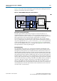
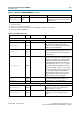
Figure 5–9 shows the order of the functions performed by the read datapath and the
frequency at which the read data is handled.
Data Capture and Resynchronization
The data capture and resynchronization registers for Arria II GX devices are
implemented in the I/O element (IOE) to achieve maximum performance. Data
capture and resynchronization is the process of capturing the read data (DQ) with the
DQS/DQSn strobes and resynchronizing the captured data to an internal
free-running full-rate clock supplied by the enhanced PLL. The resynchronization
clock is an intermediate clock whose phase shift is determined during the calibration
stage. The captured data (
rdata_p_captured
and
rdata_n_captured
) is synchronized
to the resynchronization clock (
resync_clk_2x
), refer to Figure 5–9. For Arria II GX
devices, the ALTMEMPHY instances an ALTDQ_DQS megafunction that instantiates
the required IOEs for all the DQ and DQS pins.
Data Demultiplexing
Data demultiplexing is the process of changing the SDR data into HDR data. Data
demultiplexing is required to bring the frequency of the resynchronized data down to
the frequency of the system clock, so that data from the external memory device can
ultimately be brought into the FPGA controller clock domain. Before data capture, the
data is DDR and n-bit wide. After data capture, the data is SDR and 2n-bit wide. After
data demuxing, the data is HDR of width 4n-bits wide. The system clock frequency is
half the frequency of the memory clock. Demultiplexing is achieved using a dual-port
memory with a 2n-bit wide write-port operating on the resynchronization clock (SDR)
and a 4n-bit wide read-port operating on the PHY clock (HDR). The basic principle of
operation is that data is written to the memory at the SDR rate and read from the
memory at the HDR rate while incrementing the read- and write-address pointers. As
the SDR and HDR clocks are generated, the read and write pointers are continuously
incremented by the same PLL, and the 4n-bit wide read data follows the 2n-bit wide
write data with a constant latency
Figure 5–9. DDR3 SDRAM Read Datapath in Arria II GX Devices
SDR SDR/HDR
DDR
DQ
DQ
Data Capture
IOE
DQ
DQ
DQ
Data Resynchronization
IOE
Data Demux and Alignment
RAM Block
wr_data[2n]
rd_data[4n]
wr_clk rd_clk
FIFO
phy_clk_1x
resync_clk_2x
DQ[n]
DQS