
User guide


5–18 Chapter 5: Functional Description—ALTMEMPHY
Block Description
External Memory Interface Handbook Volume 3 December 2010 Altera Corporation
Section II. DDR3 SDRAM Controller with ALTMEMPHY IP User Guide
Read Datapath
This topic discusses the read datapath.
Arria II GX Devices
The read datapath logic captures data sent by the memory device and subsequently
aligns the data back to the system clock domain. The read datapath for DDR3 SDRAM
consists of the following three main blocks:
■ Data capture
■ Data resynchronization
■ Data demultiplexing and alignment
As the DQS/DQSn signal is not continuous, the PHY also has postamble protection
logic to ensure that any glitches on the DQS input signals at the end of the read
postamble time do not cause erroneous data to be captured as a result of postamble
glitches.
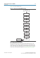
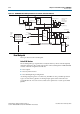
Figure 5–8. ALTMEMPHY Reset Management Block for Stratix IV and Stratix III Devices
PLL
Q
Q
SET
CLR
D
Q
Q
SET
CLR
D
Q
Q
SET
CLR
D
Q
Q
SET
CLR
D
Q
Q
SET
CLR
D
Q
Q
SET
CLR
D
soft_reset_n
global_reset_n
pll_ref_clk
phy_clk_out
reset_request_n
phy_internal_reset_n
areset
(active HIGH)
pll_reconfig_reset_ams_n
pll_reconfig_reset_ams_n_r
refclk
c0
locked
reset_master_ams
global_pre_clear
Reset
Pipes
PHY resets
pll_reset
pll_locked
Internal reset signal
signal for the
PLL clock-domain
crossing registers
Optional
reset_
request_n
edge detect and
reset counter, not
created by the PHY
clk_divider_reset_n
clk
divider
circuit
phy_clk
reset_n
scan
_
clk
clk_div_reset_ams_n
clk_div_reset_ams_n_r
pll_reconfig_reset_n
global_or_soft_reset_n
Another
system
clock