
User guide


5–16 Chapter 5: Functional Description—ALTMEMPHY
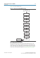
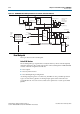
Block Description
External Memory Interface Handbook Volume 3 December 2010 Altera Corporation
Section II. DDR3 SDRAM Controller with ALTMEMPHY IP User Guide
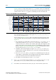
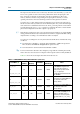
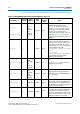
Table 5–2 shows the PLL outputs and their usage for Stratix III and Stratix IV devices.
Table 5–2. DDR3 SDRAM Clocking Stratix IV and Stratix III Devices (Part 1 of 2)
Clock Name (1)
Postscale
Counter
Phase
(Degrees)
Clock
Rate
Clock
Network
Type
Notes
phy_clk_1x
and
aux_half_rate_clk
C0
–40°
(with
leveling)
30°
(without
leveling)
Half-Rate Global
The only clock parameterizable for the
ALTMEMPHY megafunction. With
phy_clk_1x
the sequencer generates
another
sc_clk_dp
clock with this clock
that programs the scan chains of the I/O
elements. For more information on
changing the clock network type, refer to the
ALTMEMPHY Design Tutorials section in
volume 6 of the External Memory Interface
Handbook.
mem_clk_2x
C1 0 Full-Rate Special
Generates
mem_clk
that provides the
reference clock for the DLL. A dedicated
routing resource exists from the PLL to the
DLL, which you select with the regional
routing resource for the
mem_clk
using the
following attribute in the HDL:
(-name global_signal dual_regional
_clock;
-to dll~DFFIN
-name global_signal off)
. If you use
an external DLL, apply this attribute
similarly to the external DLL.
aux_full_rate_clk
C2
0°
(with
leveling)
60°
(without
leveling)
Full-Rate None
A copy of
mem_clk_2x
that you can use in
other parts of your design.
write_clk_2x
C3
0°
(with
leveling)
–90°
(without
leveling)
Full-Rate Regional
This clock feeds the write leveling delay
chains that generate the DQ, DM, DQS, and
mem_clk
signals.
resync_clk_2x
C4 Calibrated Full-Rate Regional
This clock feeds the I/O clock divider that
then reads the data out of the DDIO pins. Its
phase is adjusted in the calibration process.
The design uses an inverted version of this
clock for postamble clocking.
measure_clk_1x
C5 Calibrated Half-Rate
Regional
(2)
This clock is for VT tracking. This
free-running clock measures relative phase
shifts between the internal clock(s) and
those being fed back through a mimic path.
As a result, you can track VT effects on the
FPGA and compensate for the effects.