
User guide


Chapter 5: Functional Description—ALTMEMPHY 5–15
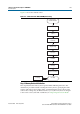
Block Description
December 2010 Altera Corporation External Memory Interface Handbook Volume 3
Section II. DDR3 SDRAM Controller with ALTMEMPHY IP User Guide
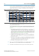
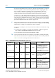
ac_clk_2x
C3
–90°
Full-Rate Global
Address and command clock.
The
ac_clk_2x
clock is derived
from either
mem_clk_2x
(when
you choose 0° or 180° phase
shift) or
write_clk_2x
(when you
choose 90° or 270° phase shift).
Refer to “Address and Command
Datapath” on page 5–11 for
illustrations of the address and
command clock relationship with
the
mem_clk_2x
or
write_clk_2x
signals.
cs_n_clk_2x
C3 –90° Full-Rate Global
Memory chip-select clock.
The
cs_n_clk_2x
clock is derived
from
ac_clk_2x
.
resync_clk_2x
C4 Calibrated Full-Rate Global
Clocks the resynchronization
registers after the capture
registers. Its phase is adjusted to
the center of the data valid window
across all the DQS-clocked DDIO
groups.
measure_clk_2x
C5 Calibrated Full-Rate Global
This clock is for VT tracking. This
free-running clock measures
relative phase shifts between the
internal clock(s) and those being
fed back through a mimic path. As
a result, the ALTMEMPHY
megafunction can track VT effects
on the FPGA and compensate for
the effects.
Note to Table 5–1:
(1) The
_1x
clock represents a frequency that is half of the memory clock frequency; the
_2x
clock represents the memory clock frequency.
Table 5–1. DDR3 SDRAM Clocking in Arria II GX Devices (Part 2 of 2)
Clock Name (1)
Postscale
Counter
Phase
(Degrees)
Clock Rate
Clock
Network Type
Notes