
User guide


5–14 Chapter 5: Functional Description—ALTMEMPHY
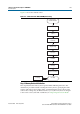
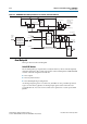
Block Description
External Memory Interface Handbook Volume 3 December 2010 Altera Corporation
Section II. DDR3 SDRAM Controller with ALTMEMPHY IP User Guide
The input clock to the PLL does not have any other fan-out to the PHY, so you do not
have to use a global clock resource for the path between the clock input pin to the
PLL. You must use the PLL located in the same device quadrant or side as the
memory interface and the corresponding clock input pin for that PLL, to ensure
optimal performance and accurate timing results from the Quartus II software.
You must choose a PLL and PLL input clock pin that are located on the same side of
the device as the memory interface to ensure minimal jitter. Also, ensure that the input
clock to the PLL is stable before the PLL locks. If not, you must perform a manual PLL
reset (by driving the
global_reset_n
signal low) and relock the PLL to ensure that the
phase relationship between all PLL outputs is properly set.
1 If the design cascades PLLs, the source (upstream) PLL should have a low-bandwidth
setting, and the destination (downstream) PLL should have a high-bandwidth setting.
Adjacent PLLs cascading is recommended to reduce clock jitter.
Cross-device cascading PLLs are only allowed in Stratix III devices with the following
conditions:
■ Upstream PLL: 0.59 MHz =< upstream PLL bandwidth < 1 MHz. The upstream
PLL should use the With No Compensation operation mode.
■ Downstream PLL: downstream PLL bandwidth > 2 MHz.
f For more information about the VCO frequency range and the available phase shifts,
refer to the Clock Networks and PLLs chapter in the respective device family handbook.
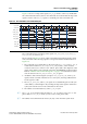
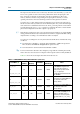
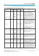
Table 5–1 shows the clock outputs that Arria II GX devices use.
Table 5–1. DDR3 SDRAM Clocking in Arria II GX Devices (Part 1 of 2)
Clock Name (1)
Postscale
Counter
Phase
(Degrees)
Clock Rate
Clock
Network Type
Notes
phy_clk_1x
and
aux_half_rate_clk
C0 0° Half-Rate Global
The only clocks parameterizable for
the ALTMEMPHY megafunction.
These clocks also feed into a
divider circuit to provide the PLL
scan_clk
signal (for
reconfiguration) that must be lower
than 100 MHz.
mem_clk_2x
and
aux_full_rate_clk
C1 0° Full-Rate Global
This clock is for clocking DQS and
as a reference clock for the
memory devices.
mem_clk_1x
C2 0° Half-Rate Global
This clock is for clocking DQS and
as a reference clock for the
memory devices.
write_clk_2x
C3 –90° Full-Rate Global
This clock is for clocking the data
out of the DDR I/O (DDIO) pins in
advance of the DQS strobe (or
equivalent). As a result, its phase
leads that of the
mem_clk_2x
by
90°.