
User guide


Chapter 5: Functional Description—ALTMEMPHY 5–13
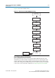
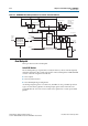
Block Description
December 2010 Altera Corporation External Memory Interface Handbook Volume 3
Section II. DDR3 SDRAM Controller with ALTMEMPHY IP User Guide
Stratix III and Stratix IV Devices
The address and command clock is one of the PLL dedicated clock outputs whose
phase can be adjusted to meet the setup and hold requirements of the memory clock.
The Stratix III address and command clock,
ac_clk_1x
, is half rate. The command and
address pins use the DDIO output circuitry to launch commands from either the
rising or falling edges of the clock. The chip select (
mem_cs_n
), clock enable (
mem_cke
),
and
mem_odt
pins are enabled on one memory clock cycle basis and can be launched
from either the rising or falling edge of the
ac_clk_1x
signal, while the address and
other command pins are enabled for two memory clock cycles and can also be
launched from either the rising or falling edge of
ac_clk_1x
signal. It is the
responsibility of the controller to maintain the relative timing of the signals.
The DDR3 SDRAM PHY generates a write latency output
ctl_wlat
that indicates the
number of
ctl_clk
cycles between the write command being issued,
ctl_cs_n
asserted, and
ctl_dqs_burst
being asserted. This
ctl_wlat
signal is only valid when
calibration has been successfully completed by the ALTMEMPHY sequencer and does
not change at any point during normal user mode operation. The value on
ctl_wlat
includes the effect of the following as determined during calibration:
■ CAS write latency (CWL)
■ Additive latency
■ Datapath latencies and relative phases
■ Board and memory module layout
■ Address and command path latency and 1T register setting which is dynamically
set up to take into account any leveling effects
Clock and Reset Management
The clocking and reset block is responsible for clock generation, reset management,
and phase shifting of clocks. It also has control of clock network types that route the
clocks, which is handled in the <variation_name>
_alt_mem_phy_clk_reset
module in
the <variation_name>_alt_mem_phy.v/.vhd file.
Clock Management
The clock management feature allows the ALTMEMPHY megafunction to work out
the optimum phase during calibration, and to track voltage and temperature variation
relies on phase shifting the clocks relative to each other.
1 Certain clocks require phase shifting during the ALTMEMPHY megafunction
operation.
You can implement clock management circuitry using PLLs and DLLs.
The ALTMEMPHY MegaWizard Plug-In Manager automatically generates an
ALTPLL megafunction instance. The ALTPLL megafunction generates the different
clock frequencies and relevant phases used within the ALTMEMPHY megafunction.
The available device families have different PLL capabilities. The minimum PHY
requirement is to have 16 phases of the highest frequency clock. The PLL uses With
No Compensation option to minimize jitter. Changing the PLL compensation to a
different operation mode may result in inaccurate timing results.