
User guide


5–12 Chapter 5: Functional Description—ALTMEMPHY
Block Description
External Memory Interface Handbook Volume 3 December 2010 Altera Corporation
Section II. DDR3 SDRAM Controller with ALTMEMPHY IP User Guide
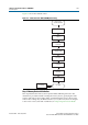
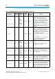
Figure 5–6 shows a 1T chip select signal (
mem_cs_n
), which is active low, and disables
the command in the memory device. All commands are masked when the chip-select
signal is inactive. The
mem_cs_n
signal is considered part of the command code.
The command interface is made up of the signals
mem_ras_n
,
mem_cas_n
,
mem_we_n
,
mem_cs_n
,
mem_cke
, and
mem_odt
.
The waveform in Figure 5–6 shows a NOP command followed by five back-to-back
write commands. The following sequence corresponds with the numbered items in
Figure 5–6.
1. The commands are asserted either on the rising edge of
ac_clk_2x
. The
ac_clk_2x
is derived from either
mem_clk_2x
(0° ),
write_clk_2x
(270° ), or the inverted
variations of those two clocks (for 180
° and 90° phase shifts). This depends on the
setting of the address and command clock in the ALTMEMPHY parameter editor.
Refer to “Address and Command Datapath” on page 5–11 for illustrations of this
clock in relation to the
mem_clk_2x
or
write_clk_2x
signals.
2. All address and command signals (except for
mem_cs_ns
,
mem_cke
, and
mem_odt
signals) remain asserted on the bus for two clock cycles, allowing sufficient time
for the signals to settle.
3. The
mem_cs_n
,
mem_cke
, and
mem_odt
signals are asserted during the second cycle
of the address/command phase. By asserting the chip-select signal in alternative
cycles, back-to-back read or write commands can be issued.
4. The address is incremented every other
ac_clk_2x
cycle.
1 The
ac_clk_2x
clock is derived from either
mem_clk_2x
(when you choose 0° or 180°
phase shift) or
write_clk_2x
(when you choose 90° or 270° phase shift).
1 The address and command clock can be 0, 90, 180, or 270° from the system clock.
Figure 5–6. Arria II GX Address and Command Datapath
Command
ac_clk_2x
mem_addr
mem_ba
mem_cs_n
mem_ras_n
mem_cas_n
mem_we_n
mem_dq
[1] [2]
[4] [4] [4]
NOP
NOP
[3]
mem-dqs
PHY Command Outputs
[3]
[1]
NOP
NOP
PCH ACT
WR
0000
00
0001
0000
0004
0008
000C
0010 0000