
User guide


5–8 Chapter 5: Functional Description—ALTMEMPHY
Block Description
External Memory Interface Handbook Volume 3 December 2010 Altera Corporation
Section II. DDR3 SDRAM Controller with ALTMEMPHY IP User Guide
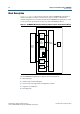
■ Banks 0, 1, and 2
■ Row 0
■ All columns
Bank 0 is written to for the block training pattern and clock cycle calibration (
DQ_1T
and
AC_1T
). Bank 1 is written to for write deskew (DQ). Bank 2 is written to for write
deskew (DM). For each bank, only row 0 is accessed. The number of columns accessed
can vary, but you should avoid writing to all columns in these banks and row 0.
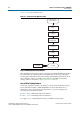
The calibration process for the DDR3 SDRAM PHY with leveling includes the
following steps:
■ “Step 1: Memory Device Initialization”
■ “Step 2: Write Leveling”
■ “Step 3: Write Training Patterns”
■ “Step 4: Read Resynchronization”
■ “Step 5: Address and Command Path Clock Cycle”
■ “Step 7: Write Clock Path Setup”
■ “Step 8: Prepare for User Mode”
1 No steps can be bypassed. Therefore, even if you are using only one DDR3 SDRAM
DIMM, all the calibration sequences are performed.
The calibration assumes that the skew for all the DQS launch times is one clock period
maximum.
The VT tracking portion of the DDR3 SDRAM sequencer is similar to that of the DDR
or DDR2 SDRAM sequencer.