
User guide


Chapter 5: Functional Description—ALTMEMPHY 5–7
Block Description
December 2010 Altera Corporation External Memory Interface Handbook Volume 3
Section II. DDR3 SDRAM Controller with ALTMEMPHY IP User Guide
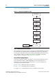
1 The mimic path in Arria II GX, Stratix III and Stratix IV devices is similar to
Figure 5–3. The only difference is that the
mem_clk[0]
pin is generated by DDIO
register;
mem_clk_n[0]
is generated by signal splitter.
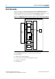
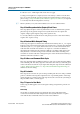
DDR3 SDRAM With Leveling
The calibration process for the DDR3 SDRAM PHY (with leveling) assumes an
interface in an unbuffered DIMM format, where the clock uses a fly-by termination,
refer to Figure 5–4.
With fly-by termination, each DDR3 SDRAM device on the DIMM sees the CK/CKn
edges at different times. Therefore, the sequencer must adjust the clock to launch the
DQS/DQSn and DQ signals so that it is appropriately aligned to the CK/CKn signals
on each device.
The DDR3 SDRAM leveling sequencer during calibration writes to the following
locations:
Figure 5–3. Mimic Path
mem_clk[0]
datain
1
ddiodatain
0
outclk
ALTPLL
mem_clk_2x
measure_clk
mimic_data_in
measure_clk
alt_mem_phy_mimic
combout
Figure 5–4. DDR3 SDRAM Unbuffered Module Clock Topology
DQS/DQ
DQS/DQDQS/DQ
DQS/DQ
DQS/DQ
DQS/DQ
CK/CK#
DQS/DQ DQS/DQ