
User guide

Chapter 4: Compiling and Simulating 4–3
Compiling the Design
December 2010 Altera Corporation External Memory Interface Handbook Volume 3
Section II. DDR3 SDRAM Controller with ALTMEMPHY IP User Guide
■ Alternatively, to change the pin names that do not match the design, you can add a
prefix to your pin names by performing the following steps:
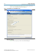
a. On the Assignments menu, click Pin Planner.
b. On the Edit menu, click Create/Import Megafunction.
c. Select Import an existing custom megafunction and navigate to
<variation name>.ppf.
d. Type the prefix you want to use in Instance name. For example, change
mem_addr to core1_mem_addr.
3. Set the top-level entity to the top-level design.
a. On the File menu, click Open.
b. Browse to your SOPC Builder system top-level design or <variation
name>_example_top if you are using MegaWizard Plug-In Manager, and click
Open.
c. On the Project menu, click Set as Top-Level Entity.
4. Assign the DQ and DQS pin locations.
a. You should assign pin locations to the pins in your design, so the Quartus II
software can perform fitting and timing analysis correctly.
b. Use either the Pin Planner or Assignment Editor to assign the clock source pin
manually. Also choose which DQS pin groups should be used by assigning
each DQS pin to the required pin. The Quartus II Fitter then automatically
places the respective DQ signals onto suitable DQ pins within each group.
1 To avoid no-fit errors when you compile your design, ensure that you place
the
mem_clk
pins to the same edge as the
mem_dq
and
mem_dqs
pins, and set
an appropriate I/O standard for the non-memory interfaces, such as the
clock source and the reset inputs, when assigning pins in your design. For
example, for DDR3 SDRAM select 1.5 V. Also select in which bank or side
of the device you want the Quartus II software to place them.
The ×4 DIMM has the following mapping between DQS and DQ pins:
■ DQS[0] maps to DQ[3:0]
■ DQS[1] maps to DQ[7:4]
■ DQS[2] maps to DQ[11:8]
■ DQS[3] maps to DQ[15:12]
The DQS pin index in other ×4 DIMM configurations typically increases
sequentially with the DQ pin index (DQS[0]: DQ[3:0]; DQS[1]: DQ[7:4]; DQS[2]:
DQ[11:8])
5. For Stratix III and Stratix IV designs, if you are using advanced I/O timing, specify
board trace models in the Device & Pin Options dialog box. If you are using any
other device and not using advanced I/O timing, specify the output pin loading
for all memory interface pins.