
User guide


Chapter 3: Parameter Settings 3–9
ALTMEMPHY Parameter Settings
December 2010 Altera Corporation External Memory Interface Handbook Volume 3
Section II. DDR3 SDRAM Controller with ALTMEMPHY IP User Guide
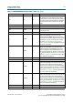
t
WTR
1–6 t
CK
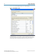
Minimum write-to-read command delay. The controller
waits for this period of time after the end of a write
command before issuing a subsequent read command
to the same bank. This timing parameter is specified in
clock cycles and the value is rounded off to the next
integer.
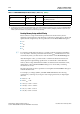
t
AC
0–750 ps DQ output access time.
t
DQSCK
50–750 ps DQS output access time from CK/CK# signals.
t
DQSQ
50–500 ps
The maximum DQS to DQ skew; DQS to last DQ valid,
per group, per access.
t
DQSS
0–0.3 t
CK
Positive DQS latching edge to associated clock edge.
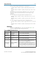
t
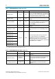
DH
10–600 ps
DQ and DM input hold time relative to DQS, which has a
derated value depending on the slew rate of the
differential DQS and DQ/DM signals. Ensure that you
are using the correct number and that the value entered
is referenced to V
REF
(dc), not V
IH
(dc) min or V
IL
(dc)
max. Refer to “Derating Memory Setup and Hold
Timing” on page 3–10 for more information about how
to derate this specification.
t
DS
10–600 ps
DQ and DM input setup time relative to DQS, which has
a derated value depending on the slew rate of the
differential DQS signals and DQ/DM signals. Ensure
that you are using the correct number and that the
value entered is referenced to V
REF
(dc), not V
IH
(ac) min
or V
IL
(ac) max. Refer to “Derating Memory Setup and
Hold Timing” on page 3–10 for more information about
how to derate this specification.
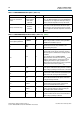
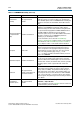
t
DSH
0.1–0.5 t
CK
DQS falling edge hold time from CK.
t
DSS
0.1–0.5 t
CK
DQS falling edge to CK setup.
t
IH
50–1000 ps
Address and control input hold time, which has a
derated value depending on the slew rate of the CK and
CK# clocks and the address and command signals.
Ensure that you are using the correct number and that
the value entered is referenced to
VREF
(dc), not V
IH
(dc)
min or V
IL
(dc) max. Refer to “Derating Memory Setup
and Hold Timing” on page 3–10 for more information
about how to derate this specification.
t
IS
65–1000 ps
Address and control input setup time, which has a
derated value depending on the slew rate of the CK and
CK# clocks and the address and command signals.
Ensure that you are using the correct number and that
the value entered is referenced to V
REF
(dc), not V
IH
(ac)
min or V
IL
(ac) max. Refer to “Derating Memory Setup
and Hold Timing” on page 3–10 for more information
about how to derate this specification.
t
QHS
0–700 ps The maximum data hold skew factor.
t
QH
0.1–0.6 t
CK
DQ output hold time.
Table 3–5. DDR3 SDRAM Timing Parameter Settings (Part 2 of 3) (Note 1)
Parameter Name Range Units Description