
User guide


Chapter 3: Parameter Settings 3–5
ALTMEMPHY Parameter Settings
December 2010 Altera Corporation External Memory Interface Handbook Volume 3
Section II. DDR3 SDRAM Controller with ALTMEMPHY IP User Guide
Table 3–3 through Table 3–5 describe the DDR3 SDRAM parameters available for
memory attributes, initialization options, and timing parameters.
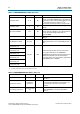
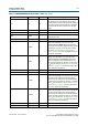
Table 3–3. DDR3 SDRAM Attributes Settings (Part 1 of 2)
Parameter Name Range (1) Units Description
Output clock pairs from FPGA 1–6 pairs
Defines the number of differential clock pairs driven from
the FPGA to the memory. Memory clock pins use the
signal splitter feature in Arria II GX, Stratix III, and
Stratix IV devices for differential signaling.
The ALTMEMPHY parameter editor displays an error on
the bottom of the window if you choose more than one
for DDR3 SDRAM interfaces.
Total Memory chip selects 1, 2, 4, or 8 bits
Sets the number of chip selects in your memory
interface. The number of chip selects defines the depth of
your memory. You are limited to the range shown as the
local side binary encodes the chip select address.
Memory interface DQ width 4–288 bits
Defines the total number of DQ pins on the memory
interface. If you are interfacing with multiple devices,
multiply the number of devices with the number of DQ
pins per device. Even though the GUI allows you to
choose 288-bit DQ width, DDR3 SDRAM variations are
only supported up to 80-bit width due to restrictions in
the board layout which affects timing at higher data
width. Furthermore, the interface data width is limited by
the number of pins on the device. For best performance,
have the whole interface on one side of the device.
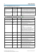
Mirror addressing — —
On multiple rank DDR3 SDRAM DIMMs address signals
are routed differently to each rank; referred to in the
JEDEC specification as address mirroring.
Enter ranks with mirrored addresses in this field. There is
one bit per chip select. For example, for four chip selects,
enter 1011 to mirror the address on chip select #3, #1,
and #0.
Register Control Word 0–15
for Registered DIMMs
—bits
Register Control Word values for the DDR3 registered
DIMMs. The values are available in the memory data
sheet of the respective registered DIMMs.
Memory vendor
Elpida, JEDEC,
Micron,
Samsung, Hynix,
Nanya, other
—
Lists the name of the memory vendor for all supported
memory standards.
Memory format
Discrete Device,
Unbuffered
DIMM
—
Specifies whether you are interfacing with devices or
modules. SODIMM and MicroDIMM are supported under
unbuffered DIMMs. The ALTMEMPHY megafunction for
DDR3 SDRAM interfaces does not support registered
DIMM format. Arria II GX devices only support DDR3
SDRAM components without leveling, for example,
Discrete Device memory format.
Maximum memory frequency
See the memory
device datasheet
MHz Sets the maximum frequency supported by the memory.
Column address width 10–12 bits
Defines the number of column address bits for your
interface.