
User guide

2–10 Chapter 2: Getting Started
HardCopy Device Migration Guidelines
External Memory Interface Handbook Volume 3 December 2010 Altera Corporation
Section II. DDR3 SDRAM Controller with ALTMEMPHY IP User Guide
HardCopy Device Migration Guidelines
In HardCopy III and HardCopy IV designs where higher core performance is
required and I/O performance is not a limiting factor, you can prototype your
HardCopy design in a faster speed grade companion FPGA. However, this practice
introduces some restrictions and limitations. For example, if you target a HardCopy
device with an FPGA device as a prototype, the Quartus II Fitter restricts the VCO
operating range of the PLL to the mid speed grade frequency, regardless of the actual
speed grade of the FPGA that the design is targeting.
Enabling Hardcopy Migration Performance Improvement with ALTMEMPHY
You can achieve improved performance when implementing an IP core for use with a
HardCopy device by first generating your IP for a lower-speed FPGA to achieve
optimal implementation, and then compiling your design for the higher-speed FPGA
companion to your HardCopy device. This process is summarized below:
1. Generate your IP core, targeting a mid-speed grade FPGA.
2. Compile your design, targeting a faster speed grade FPGA.
The following sections discuss the above steps in greater detail.
Generating Your IP Core For a Mid-speed Grade FPGA
When you parameterize and generate your controller using the ALTMEMPHY
parameter editor, the PHY, PLL, and DLL are parameterized and generated together
with the controller logic. Robust calibration and operation require that all of these
blocks operate with matched settings. To ensure that you have matched settings, any
IP that includes hard blocks should be generated in the MegaWizard Plug-In Manager
targeting a mid-speed grade FPGA rather than the C2 speed grade. By targeting a
mid-speed grade FPGA, you ensure that any process-dependant settings are
appropriately restricted when the IP core is generated, thereby maintaining a
consistent post-fit implementation throughout the compilation process. You can then
compile the design for either a mid- or high-speed grade FPGA, depending on
whether you want speed enhancements.
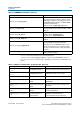
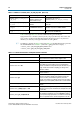
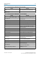
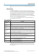
The following example illustrates this situation. Table 2–7 shows the key parameters.
Table 2–7. PHY Sequencer Parameters (Part 1 of 2)
Parameter Setting
DLL_DELAY_BUFFER_MODE HIGH
DLL_DELAY_CHAIN_LENGTH 10
DQS_DELAY_CTL_WIDTH 6
DQS_OUT_MODE DELAY_CHAIN2
DQS_PHASE 7200
DQS_PHASE_SETTING 2
MEM_IF_CLK_PS 3300
MEM_IF_CLK_PS_STR 3300 ps
MEM_IF_MR_0 4641