
User guide


Chapter 9: Timing Diagrams 9–23
DDR3 High-Performance Controllers II
December 2010 Altera Corporation External Memory Interface Handbook Volume 3
Section II. DDR3 SDRAM Controller with ALTMEMPHY IP User Guide
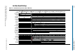
The following sequence corresponds with the numbered items in Figure 9–12:
1. The user logic requests the first read by asserting the
local_read_req
signal, and
the size and address for this read. In this example, the request is a burst of length
of 2 to the local address
0×0000810
. This local address is mapped to the following
memory address in half-rate mode:
mem_row_address = 0×0001
mem_col_address = 0×0010<<2 = 0×0040
mem_bank_address = 0×00
2. When the command queue is full, the controller deasserts the
local_ready
signal
to indicate that the controller has not accepted the command. The user logic must
keep the read request, size, and address signal until the
local_ready
signal is
asserted again.
3. The user logic asserts a second
local_read_req
signal with a size of 2 and address
of
0×0000912
.
4. The controller issues the first read memory command and address signals to the
ALTMEMPHY megafunction for it to send to the memory device.
5. The ALTMEMPHY megafunction issues the read command to the memory and
captures the read data from the memory.
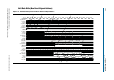
Half-Rate Write With Gaps
Figure 9–13. Half-Rate Write Operation for HPC II—With Gaps
phy_clk
local_address[25:0]
Local Interface
local_size[4:0]
local_ready
local_burstbegin
local_be[3:0]
local_write_req
local_wdata[31:0]
afi_addr[27:0]
Controller - AFI
afi_ba[5:0]
afi_cs_n[3:0]
AFI Command[2:0]
afi_dm[3:0]
afi_wlat[4:0]
afi_dqs_burst[0]
afi_dqs_burst[1]
afi_wdata[31:0]
afi_wdata_valid[1:0]
mem_cke[1:0]
AFI Memory Interface
mem_clk
mem_ba[2:0]
mem_addr[13:0]
mem_cs_n[0]
Mem Command[2:0]
mem_dqs
mem_dm
mem_dq[7:0]
mem_odt[1:0]
0000F1C
2
AABBCCDD EEFF0011 AABBCCDD
0000000
40C1030
3F
F
B
F
WR NOPNOP
F 0 F
EEFF0011 AABBCCDD EEFF0011
0
3 0
7
1030
WR NOPNOP
00 DD CC BB AA 11 00 FF EE 00
[1] [6]
[2] [5] [3][4]