
User guide


Chapter 9: Timing Diagrams 9–13
DDR3 High-Performance Controllers II
December 2010 Altera Corporation External Memory Interface Handbook Volume 3
Section II. DDR3 SDRAM Controller with ALTMEMPHY IP User Guide
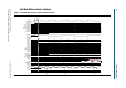
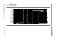
The following sequence corresponds with the numbered items in Figure 9–7:
1. The write leveling stage.
2. The write leveling coarse phase sweep.
3. Fine T9/T10 delay chain sweep.
4. The write burst training pattern.
5. Three training patterns available at different addresses—zeroes, ones, and mixed.
6. The read path setup starts with the first operation, read deskew.
7. The read path deskew increases capture margin.
8. The write deskew stage; patterns written to RAM and read back.
9. The write datapath setup; data written to DRAM to determine latency.
10. Advertise read and write latency stage.
11. Tracking setup stage to set up mimic window.
12. Calibration successful on user mode.
DDR3 High-Performance Controllers II
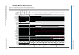
This section discusses the following timing diagrams for HPC II:
■ “Half-Rate Read (Burst-Aligned Address)”
■ “Half-Rate Write (Burst-Aligned Address)”
■ “Half-Rate Read (Non Burst-Aligned Address)”
■ “Half-Rate Write (Non Burst-Aligned Address)”
■ “Half-Rate Read With Gaps”
■ “Half-Rate Write With Gaps”
■ “Half-Rate Write Operation (Merging Writes)”
■ “Write-Read-Write-Read Operation”