
User guide


9–10 Chapter 9: Timing Diagrams
DDR3 High-Performance Controllers
External Memory Interface Handbook Volume 3 December 2010 Altera Corporation
Section II. DDR3 SDRAM Controller with ALTMEMPHY IP User Guide
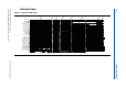
Initialization Timing
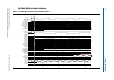
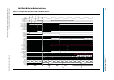
Figure 9–6. Initialization Timing for HPC
global_reset_n
pll_locked
phs_shft_busy
seq_pll_select[3:0]
seq_pll_start_reconfig
seq_pll_inc_dec_n
seq_ac_ras_n[1:0]
seq_ac_cas_n[1:0]
seq_ac_we_n[1:0]
memory_0_0.ck
memory_0_0.ck_n
memory_0_0.cke
memory_0_0.cs_n
memory_0_0.addr[13:0]
memory_0_0.ras_n
memory_0_0.cas_n
memory_0_0.we_n
memory_0_0.odt
memory_0_0.ba[2]
memory_0_0.ba[1]
memory_0_0.ba[0]
memory_0_0.rst_n
memory_0_0.dq[7:0]
memory_0_0.dqs
memory_0_0.dqs_n
memory_0_0.dm_tdqs
memory_0_1.ck
memory_0_1.ck_n
memory_0_1.cke
memory_0_1.cs_n
memory_0_1.addr[13:0]
memory_0_1.ras_n
memory_0_1.cas_n
memory_0_1.we_n
memory_0_1.odt
memory_0_1.rst_n
memory_0_1.ba[1:0]
memory_0_1.ba[0]
memory_0_1.dq[7:0]
memory_0_1.dqs
memory_0_1.dqs_n
memory_0_1.dm_tdqs
mem_dq[15:0]
mem_dqs[1:0]
mem_dqs_n[1:0]
3
3
3
[1] [2]
[3]
[3]