
User guide


Chapter 8: Latency 8–3
December 2010 Altera Corporation External Memory Interface Handbook Volume 3
Section II. DDR3 SDRAM Controller with ALTMEMPHY IP User Guide
You can separate the controller and ALTMEMPHY read data input latency into
latency that occurred in the I/O element (IOE) and latency that occurred in the FPGA
fabric.
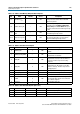
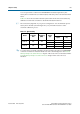
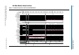
Table 8–2 shows the read and write latency derived from the write and read latency
definitions for half rate controller for Stratix III and Stratix IV devices.
1 The exact latency depends on your precise configuration. You should obtain precise
latency from simulation, but this figure may vary in hardware because of the
automatic calibration process.
f To see the latency incurred in the IOE for both read and write paths for ALTMEMPHY
variations in Stratix IV and Stratix III devices refer to the IOE figures in the External
Memory Interfaces in Stratix III Devices chapter of the Stratix III Device Handbook and the
External Memory Interfaces in Stratix IV Devices chapter of the Stratix IV Device
Handbook.
Table 8–2. Typical Latency
Device
Controller
Rate
Frequency
(MHz)
Latency
Type
Total Latency
Local Clock
Cycles
Time
(ns)
Stratix III Half 400
Read 23 115
Write 14 68
Stratix IV Half 400
Read 23 115
Write 14 68