
User guide


8–2 Chapter 8: Latency
External Memory Interface Handbook Volume 3 December 2010 Altera Corporation
Section II. DDR3 SDRAM Controller with ALTMEMPHY IP User Guide
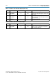
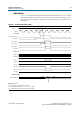
Figure 8–1 shows a typical memory interface read latency path showing read latency
from the time a
local_read_req
assertion is detected by the controller up to data
available to be read from the dual-port RAM (DPRAM) module.
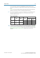
Table 8–1 shows the different stages that make up the whole read and write latency
that Figure 8–1 shows.
From Figure 8–1, the read latency in the high-performance controllers is made up of
four components:
read latency = controller latency (T1) + command output latency (T2) +
CAS latency (T3) + PHY read data input latency (T4)
Similarly, the write latency in the high-performance controllers is made up of three
components:
write latency = controller latency (T1) + write data latency (T2+T3)
Figure 8–1. Typical Latency Path
Shifted
DQS Clk
High-
Performance
Controller
PLLphy_clk
local_rdata
local_read_req
control_doing_rd
PLL
0° or 180°
PHY
FPGA Device Memory Device
Latency T3
(includes CAS
latency)
Latency T1
local_addr
mem_cs_n
mem_dq [ ]
mem_dqs [ ]
Latency T2
Address/Command Generation
Core
I/O
Alignment and
Synchronization
Capture
Shifted
DQS Clock
Resynchronization
Clock
Half-
rate
DPRAM
Read Datapath
Latency T4
mem_clk [ ]
mem_clk_n [ ]
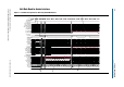
Table 8–1. High-Performance Controller Latency Stages and Descriptions
Latency Number Latency Stage Description
T1 Controller
local_read_req
or
local_write_req
signal assertion to
ddr_cs_n
signal assertion.
T2 Command Output
ddr_cs_n
signal assertion to
mem_cs_n
signal assertion.
T3 CAS or WL
Read command to DQ data from the memory or write command to DQ
data to the memory.
T4
ALTMEMPHY
read data input
Read data appearing on the local interface.
T2 + T3 Write data latency Write data appearing on the memory interface.