
User guide


Chapter 7: Functional Description—High-Performance Controller II 7–23
Register Maps Description
December 2010 Altera Corporation External Memory Interface Handbook Volume 3
Section II. DDR3 SDRAM Controller with ALTMEMPHY IP User Guide
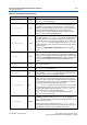
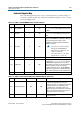
Table 7–14. Address 0x120 Memory Address Size Register 0
Bit Name Default Access Description
7:0
Column address
width
—RW
The number of column address bits for the
memory devices in your memory interface. The
range of legal values is 7-12.
15:8 Row address width — RW
The number of row address bits for the memory
devices in your memory interface. The range of
legal values is 12-16.
19:16 Bank address width — RW
The number of bank address bits for the memory
devices in your memory interface. The range of
legal values is 2-3.
23:20
Chip select address
width
—RW
The number of chip select address bits for the
memory devices in your memory interface. The
range of legal values is 0-2. If there is only one
single chip select in the memory interface, set
this bit to 0.
31:24 Reserved 0 — Reserved for future use.
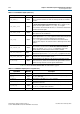
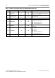
Table 7–15. Address 0x121 Memory Address Size Register 1
Bit Name Default Access Description
31:0
Data width
representation
(word)
—RW
The number of DQS bits in the memory interface.
This bit can be used to derive the width of the
memory interface by multiplying this value by the
number of
DQ
pins per
DQS
pin (typically 8).
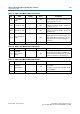
Table 7–16. Address 0x122 Memory Address Size Register 2
Bit Name Default Access Description
7:0
Chip select
representation
—RW
The number of chip select in binary
representation.
For example, a design with 2 chip selects has the
value of 00000011.
31:8 Reserved 0 — Reserved for future use.