
User guide


Chapter 7: Functional Description—High-Performance Controller II 7–21
Register Maps Description
December 2010 Altera Corporation External Memory Interface Handbook Volume 3
Section II. DDR3 SDRAM Controller with ALTMEMPHY IP User Guide
Controller Register Map
The controller register map allows you to control the memory controller settings. To
access the controller register map, connect the CSR interface signals in Table 7–6 using
the Avalon-MM protocol.
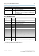
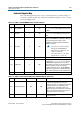
Table 7–12. Address 0x100 ALTMEMPHY Status and Control Register
Bit Name Default Access Description
0 CAL_SUCCESS — RO
This bit reports the value of the ALTMEMPHY
ctl_cal_success
output. Writing to this bit has
no effect.
1 CAL_FAIL — RO
This bit reports the value of the ALTMEMPHY
ctl_cal_fail
output. Writing to this bit has no
effect.
2 CAL_REQ 0 RW
Writing a 1 to this bit asserts the
ctl_cal_req
signal to the ALTMEMPHY megafunction. Writing a
0 to this bit deaaserts the signal, and the
ALTMEMPHY megafunction will then initiate its
calibration sequence.
c You must not use this register
during the ALTMEMPHY
megafunction calibration. You
must wait until the
CAL_SUCCESS or CAL_FAIL
register shows a value of 1.
7:3 Reserved 0 — Reserved for future use.
13:8 CLOCK_OFF 0 RW
Writing a 1 to any of the bits in this register causes
the appropriate
ctl_mem_clk_disable
signal to
the ALTMEMPHY megafunction to be asserted,
which disables the memory clock outputs. Writing
a 0 to this register deasserts the signal and
re-enables the memory clocks. The ALTMEMPHY
megafunction supports up to 6 individual memory
clocks, each bit will represent each individual clock.
30:14 Reserved 0 — Reserved for future use.
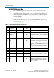
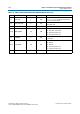
Table 7–13. Address 0x110 Controller Status and Configuration Register (Part 1 of 2)
Bit Name Default Access Description
15:0 AUTO_PD_CYCLES 0x0 RW
The number of idle clock cycles after which the
controller should place the memory into
power-down mode. The controller is considered
to be idle if there are no commands in the
command queue. Setting this register to 0
disables the auto power-down mode. The default
value of this register depends on the values set
during the generation of the design.
16 AUTO_PD_ACK 1 RO
This bit indicates that the memory is in
power-down state.