
User guide


Chapter 7: Functional Description—High-Performance Controller II 7–19
Register Maps Description
December 2010 Altera Corporation External Memory Interface Handbook Volume 3
Section II. DDR3 SDRAM Controller with ALTMEMPHY IP User Guide
ALTMEMPHY Register Map
The ALTMEMPHY register map allows you to control the memory components’
mode register settings. To access the ALTMEMPHY register map, connect the
ALTMEMPHY Debug interface signals in Table 7–8 using the Avalon-MM protocol.
After configuring the ALTMEMPHY register map, initialize a calibration request by
setting bit 2 in the CSR register map address 0x100 (Table 7–12) for the mode register
settings to take effect.
1 DDR3 SDRAM with leveling does not support the ALTMEMPHY register map. For
more information about DDR3 SDRAM with leveling, refer to “DDR3 SDRAM With
Leveling” on page 5–7.
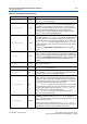
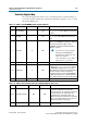
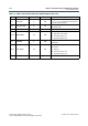
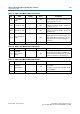
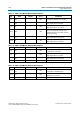
Table 7–10. Address 0x005 Mode Register 0-1 (Part 1 of 2)
Bit Name Default Access Description
2:0 Burst length 8 RO
This value is set to 8 because the DDR3 SDRAM
HPC II only supports a burst length of 8.
3BT 0 RO
This value is set to 0 because DDR3 SDRAM
SDRAM HPC II only supports sequential bursts.
6:4 CAS latency — RW
CAS latency setting. The default value for these bits
is set by the MegaWizard CAS Latency setting for
your controller instance. You must set this value in
the CSR interface register map 0x126 (Table 7–20)
as well.
7 Reserved 0 — Reserved for future use.
8 DLL 0 RW
Not used by the controller, but you can set and
programm into the memory device mode register.
11:9 Write recovery — RW
Write recovery (t
WR
) setting. The default value for
these bits is set by the MegaWizard Write Recovery
(t
WR
) setting for your controller instance. You must
set this value in CSR interface register map 0x126
(Table 7–20) as well.
12 PD 0/1 RO
This value is set to 0 because DDR3 SDRAM HPC II
only supports power-down fast exit mode.
15:13 Reserved 0 — Reserved for future use.
16 DLL 0 RW
Not used by the controller, but you can set and
program into the memory device mode register.
17 ODS 0 RW
18 RTT 0 RW
21:19 AL — RW
Additive latency setting. The default value for these
bits is set by the MegaWizard Additive Latency
setting for your controller instance. You must set
this value in CSR interface register map 0x126
(Table 7–20) as well.