
User guide


Chapter 7: Functional Description—High-Performance Controller II 7–17
Top-level Signals Description
December 2010 Altera Corporation External Memory Interface Handbook Volume 3
Section II. DDR3 SDRAM Controller with ALTMEMPHY IP User Guide
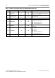
Table 7–7 shows the DDR3 SDRAM HPC II interface signals.
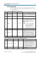
csr_rdata_valid
Output
Read data valid signal. The
csr_rdata_valid
signal indicates that valid data
is present on the read data bus.
csr_waitrequest
Output
The
csr_waitrequest
signal indicates that the HPC II is busy and not ready
to accept request signals. If the
csr_waitrequest
signal goes high in the
clock cycle when a read or write request is asserted, that request is not
accepted. If the
csr_waitrequest
signal goes low, the HPC II is then ready
to accept more requests.
Table 7–6. CSR Interface Signals (Part 2 of 2) (Part 2 of 2)
Signal Name Direction Description
Table 7–7. DDR3 SDRAM Interface Signals
Signal Name Direction Description
mem_dq[]
Bidirectional
Memory data bus. This bus is half the width of the local read and write data
busses.
mem_dqs[]
Bidirectional
Memory data strobe signal, which writes data into the DDR3 SDRAM and
captures read data into the Altera device.
mem_dqs_n[]
Bidirectional
Inverted memory data strobe signal, which is used together with the
mem_dqs
signal to improve signal integrity.
mem_clk
(1) Bidirectional Clock for the memory device.
mem_clk_n
(1) Bidirectional Inverted clock for the memory device.
mem_addr[]
Output Memory address bus.
mem_ac_parity
(2) Output
Address or command parity signal generated by the PHY and sent to the
DIMM.
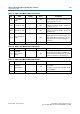
mem_ba[]
Output Memory bank address bus.
mem_cas_n
Output Memory column address strobe signal.
mem_cke[]
Output Memory clock enable signals.
mem_cs_n[]
Output Memory chip select signals.
mem_dm[]
Output Memory data mask signal, which masks individual bytes during writes.
mem_odt
Output Memory on-die termination control signal.
mem_ras_n
Output Memory row address strobe signal.
mem_we_n
Output Memory write enable signal.
parity_error_n
(2) Output
Active-low signal that is asserted when a parity error occurs and stays
asserted until the PHY is reset.
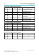
mem_err_out_n
(2) Input
Signal sent from the DIMM to the PHY to indicate that a parity error has
occured for a particular cycle.
Notes to Table 7–7:
(1) The
mem_clk
signals are output only signals from the FPGA. However, in the Quartus II software they must be defined as bidirectional (INOUT)
I/Os to support the mimic path structure that the ALTMEMPHY megafunction uses.
(2) This signal is for Registered DIMMs only.