
User guide


Chapter 7: Functional Description—High-Performance Controller II 7–9
Block Description
December 2010 Altera Corporation External Memory Interface Handbook Volume 3
Section II. DDR3 SDRAM Controller with ALTMEMPHY IP User Guide
1. The ECC logic sends a read command to the partial write address.
2. Upon receiving a return data from the memory for the particular address, the ECC
logic decodes the data, checks for errors, and then merges the corrected or correct
dataword with the incoming information.
3. The ECC logic issues a write to write back the updated data and the new ECC
code.
The following corner cases can occur:
■ A single-bit error during the read phase of the read-modify-write process. In this
case, the single-bit error is corrected first, the single-bit error counter is
incremented and then a partial write is performed to this corrected decoded data
word.
■ A double-bit error during the read phase of the read-modify-write process. In this
case, the double-bit error counter is incremented and an interrupt is issued. A new
write word is written to the location of the error. The ECC status register keeps
track of the error information.
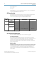
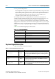
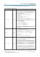
Figure 7–3 shows the partial write operation for HPC II.
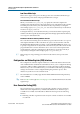
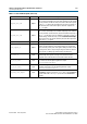
Partial Bursts
DIMMs that do not have the DM pins do not support partial bursts. You must write a
minimum of eight words to the memory at the same time.
Figure 7–4 shows the partial burst operation for HPC II.
Figure 7–3. Partial Write for HPC II
Note to Figure 7–3:
(1) R represents the internal read-back memory data during the read-modify-write process.
Figure 7–4. Partial Burst for HPC II
local_address
local_size
local_be
local_wdata
mem_dm
mem_dq
0
1
2
X1 XF
01234567
89ABCDEF
67 R R R EF CD AB 89
local_address
local_size
local_be
local_wdata
mem_dm
mem_dq
0
1
X1
01234567
67 45 23 01