
User guide


7–6 Chapter 7: Functional Description—High-Performance Controller II
Block Description
External Memory Interface Handbook Volume 3 December 2010 Altera Corporation
Section II. DDR3 SDRAM Controller with ALTMEMPHY IP User Guide
■
afi_wdata_valid
■
afi_wdata
■
afi_dm
During read, the
afi_doing_read
signal generates the
afi_rdata_valid
signal and
controls the ALTMEMPHY postamble circuit.
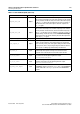
ODT Generation Logic
The ODT generation logic generates the necessary ODT signals for DDR3 SDRAM
HPC II memory devices, based on the scheme recommended by Altera.
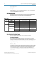
Table 7–1 shows which ODT signal on the adjacent DIMM is enabled.
User-Controlled Side-Band Signals
The user-controlled side-band signals consists of the following signals.
User-Refresh Commands
The user-refresh command enables the request to place the memory into refresh
mode. The user-refresh control takes precedence over a read or write request. You can
issue up to nine consecutive refresh commands to the selected memory chips.
However, if you enable the multi-cast write feature, the user refresh commands are
always issued to all chips.
Multi-Cast Write
The multi-cast write request signal allows you to ask the controller to send the current
write requests to all the chip selects. This means that the write data is written to all the
ranks in the system. The multi-cast write feature is useful for t
RC
mitigation where
you can cycle through chips to continuously read data without hitting t
RC
. The
multi-cast write is not supported for registered DIMM interfaces or when the ECC
logic is enabled.
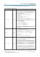
Table 7–1. ODT
DIMM
Chip Select
per DIMM
Write or Read On ODT Enabled (Write) ODT Enabled (Read)
1
Single chip select
mem_cs[0]
mem_odt[0]
— (1)
Dual chip select
mem_cs[0]
mem_odt[0]
— (1)
mem_cs[1] mem_odt[1]
— (1)
2
Single chip select
mem_cs[0]
mem_odt[0]
and
mem_odt[1] mem_odt[1]
mem_cs[1] mem_odt[0]
and
mem_odt[1] mem_odt[0]
Dual chip select
mem_cs[0]
mem_odt[0]
and
mem_odt[2] mem_odt[2]
mem_cs[1] mem_odt[1]
and
mem_odt[3] mem_odt[3]
mem_cs[2] mem_odt[0]
and
mem_odt[2] mem_odt[0]
mem_cs[3] mem_odt[1]
and
mem_odt[3] mem_odt[1]
Note to Table 7–1:
(1) The controller does not drive the ODT signals during read operation.