
User guide


Chapter 7: Functional Description—High-Performance Controller II 7–3
Block Description
December 2010 Altera Corporation External Memory Interface Handbook Volume 3
Section II. DDR3 SDRAM Controller with ALTMEMPHY IP User Guide
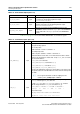
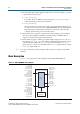
Figure 7–2 shows a block diagram of the DDR3 SDRAM HPC II architecture.
The blocks in Figure 7–2 on page 7–3 are described in the following sections.
Avalon-MM Data Slave Interface
The Avalon-MM data slave interface accepts read and write requests from the
Avalon-MM master. The width of the data,
local_wdata
and
local_rdata
, is four
times the width of the external memory.
The local address width is sized based on the memory chip, row, bank, and column
address widths. For example:
■ For multiple chip select:
width = chip bits + row bits + bank bits + column – 2
Figure 7–2. DDR3 SDRAM HPC II Architecture Block Diagram
Timer
Logic
ECC
Decoder and
Correction
ECC-enabled
ECC-enabled
Read Data
Write Data
Write Data
FIFO
PHY Register
Table
Bank
Management
Logic
Command
Queue
Command-Issuing
State Machine
Address and
Command
Decode
ECC
Encoder
Control Register
Table
Avalon-MM Data Slave Interface
Half-Rate Bridge
Avalon-MM CSR
Slave Interface
Write
Datapath
Read
Datapath
Write Data
Timing Logic
ODT
Generation
Logic
AFI