
User guide


6–20 Chapter 6: Functional Description—High-Performance Controller
Top-level Signals Description
External Memory Interface Handbook Volume 3 December 2010 Altera Corporation
Section II. DDR3 SDRAM Controller with ALTMEMPHY IP User Guide
Table 6–14 shows the DDR3 SDRAM interface signals.
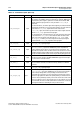
local_rdata_valid
Output
Read data valid signal. The
local_rdata_valid
signal indicates that valid
data is present on the read data bus. The timing of
local_rdata_valid
is
automatically adjusted to cope with your choice of resynchronization and
pipelining options.
local_ready
Output
The
local_ready
signal indicates that the DDR3 SDRAM HPC is ready to
accept request signals. If
local_ready
is asserted in the clock cycle that a
read or write request is asserted, that request has been accepted. The
local_ready
signal is deasserted to indicate that the DDR3 SDRAM HPC
cannot accept any more requests. The controller is able to buffer four read or
write requests.
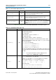
local_refresh_ack
Output
Refresh request acknowledge, which is asserted for one clock cycle every time
a refresh is issued. Even if the Enable User Auto-Refresh Controls option is
not selected,
local_refresh_ack
still indicates to the local interface that the
controller has just issued a refresh command.
local_wdata_req
Output
Write data request signal, which indicates to the local interface that it should
present valid write data on the next clock edge. This signal is only required
when the controller is operating in Native interface mode.
local_powerdn_ack
Output
Power-down request acknowledge signal. This signal is asserted and
deasserted in response to the
local_powerdn_req
signal from the user.
local_self_rfsh_ack
Output
Self refresh request acknowledge signal. This signal is asserted and
deasserted in response to the
local_self_rfsh_req
signal from the user.
Table 6–13. Local Interface Signals (Part 4 of 4)
Signal Name Direction Description
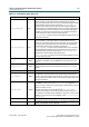
Table 6–14. DDR3 SDRAM Interface Signals
Signal Name Direction Description
mem_dq[]
Bidirectional
Memory data bus. This bus is half the width of the local read and write data
busses.
mem_dqs[]
Bidirectional
Memory data strobe signal, which writes data into the DDR3 SDRAM and
captures read data into the Altera device.
mem_clk
(1) Bidirectional Clock for the memory device.
mem_clk_n
(1) Bidirectional Inverted clock for the memory device.
mem_a[]
Output Memory address bus.
mem_ba[]
Output Memory bank address bus.
mem_cas_n
Output Memory column address strobe signal.
mem_cke[]
Output Memory clock enable signals.
mem_cs_n[]
Output Memory chip select signals.
mem_dm[]
Output Memory data mask signal, which masks individual bytes during writes.
mem_odt[]
Output Memory on-die termination control signal.
mem_ras_n
Output Memory row address strobe signal.
mem_reset_n
Output Memory reset signal.
mem_we_n
Output Memory write enable signal.
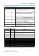
Note to Table 6–14:
(1) The
mem_clk
signals are output only signals from the FPGA. However, in the Quartus II software they must be defined as bidirectional (INOUT)
I/Os to support the mimic path structure that the ALTMEMPHY megafunction uses.