
User guide


6–16 Chapter 6: Functional Description—High-Performance Controller
Top-level Signals Description
External Memory Interface Handbook Volume 3 December 2010 Altera Corporation
Section II. DDR3 SDRAM Controller with ALTMEMPHY IP User Guide
■ Address pin operation
The example driver generates a series of write and read requests starting with an
all-zeros pattern, a walking-one pattern, a walking-zero pattern, and ending with
an all-zeros pattern. This test checks to make sure that all the individual address
bits are operating correctly. You can skip this test by setting the
test_addr_pin_on
signal to logic zero.
■ Low-power mode operation
The example driver requests that the controller place the memory into
power-down and self-refresh states, and hold it in those states for the amount of
time specified by the
COUNTER_VALUE
signal. You can vary this value to adjust the
duration the memory is kept in the low-power states. This test is only available if
your controller variation enables the low-power mode option.
The example driver has four outputs that allow you to observe which tests are
currently running and if the tests are passing. The pass not fail (
pnf
) signal goes low
once one or more errors occur and remains low. The pass not fail per byte
(
pnf_per_byte
) signal goes low when there is incorrect data in a byte but goes back
high again once correct data is observed in the following byte. The
test_status
signal
indicates the test that is currently running, allowing you to determine which test has
failed. The
test_complete
signal goes high for a single clock cycle at the end of the set
of tests.
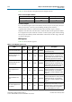
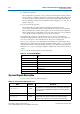
Table 6–11 shows the bit mapping for each test status.
Top-level Signals Description
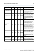
Table 6–12 shows the clock and reset signals.
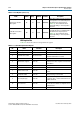
Table 6–11. Test Status[] Bit Mapping
Bit Test
0 Sequential address test
1 Incomplete write test
2 Data mask pin test
3 Address pin test
4 Power-down test
5 Self-refresh test
6 Auto precharge test
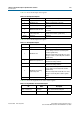
Table 6–12. Clock and Reset Signals (Part 1 of 2)
Name Direction Description
global_reset_n
Input
The asynchronous reset input to the controller. All other reset signals
are derived from resynchronized versions of this signal. This signal
holds the complete ALTMEMPHY megafunction, including the PLL, in
reset while low.
pll_ref_clk
Input The reference clock input to PLL.
soft_reset_n
Input
Edge detect reset input intended for SOPC Builder use or to be
controlled by other system reset logic. It is asserted to cause a
complete reset to the PHY, but not to the PLL used in the PHY.