
User guide


6–6 Chapter 6: Functional Description—High-Performance Controller
Block Description
External Memory Interface Handbook Volume 3 December 2010 Altera Corporation
Section II. DDR3 SDRAM Controller with ALTMEMPHY IP User Guide
■ Latency:
■ Maximum of 1 or 2 clock delay during writes
■ Minimum 1 or 3 clock delay during reads
■ Detects and corrects all single-bit errors. Also the ECC logic sends an interrupt
when the user-defined threshold for a single-bit error is reached.
■ Detects all double-bit errors. Also, the ECC logic counts the number of double-bit
errors and sends an interrupt when the user-define threshold for double-bit error
is reached.
■ Accepts partial writes
■ Creates forced errors to check the functioning of the ECC logic
■ Powers up to a ready state
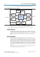
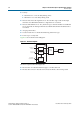
Figure 6–3 shows the ECC block diagram.
The ECC comprises the following blocks:
■ The encoder—encodes the 64-bit message to a 72-bit codeword
■ The decoder-corrector—decodes and corrects the 72-bit codeword if possible
Figure 6–3. ECC Block Diagram
Decoder-
Corrector
ECC
Controller
Encoder
Write
Message
N x 64 Bits
ECC
Write
Codeword
N x 72 Bits
Read
Message
N x 64 Bits
32 Bits
Read
Codeword
N x 72 Bits
N x 72 Bits
DDR or DDR2
SDRAM
Memory
Controller
To Local
Interface
From Local
Interface
To and From
Local Interface