
User guide

Device Transceiver Layout
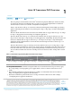
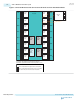
Figure 1-1: Arria 10 FPGA Architecture Block Diagram
The transceiver channels are placed on the left side periphery in most Arria 10 devices. For larger Arria 10
devices, additional transceiver channels are placed on the right side periphery.
Core Logic Fabric
M20K Internal Memory Blocks
Transceiver Channels
Hard IP Per Transceiver: Standard PCS, PCIe Gen3 PCS, Enhanced PCS
PCI Express Gen3 Hard IP
PLLs
M20K Internal Memory Blocks
PCI Express Gen3 Hard IP
Variable Precision DSP Blocks
I/O PLLs
Hard Memory Controllers, General-Purpose I/O Cells, LVDS
M20K Internal Memory BlocksM20K Internal Memory Blocks
Variable Precision DSP Blocks
Core Logic Fabric
I/O PLLs
Hard Memory Controllers, General-Purpose I/O Cells, LVDS
M20K Internal Memory BlocksM20K Internal Memory Blocks
Variable Precision DSP Blocks
Transceiver Channels
PCI Express Gen3 Hard IP PCI Express Gen3 Hard IP
PLLs
Hard IP Per Transceiver: Standard PCS, PCIe Gen3 PCS, Enhanced PCS
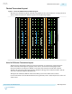
Arria 10 GX Device Transceiver Layout
The largest Arria 10 GX device includes 96 transceiver channels. A column array of eight transceiver
banks on the left and the right side periphery of the device is shown in the following figure. Each
transceiver bank has six transceiver channels. Some devices have transceiver banks with only three
channels. The transceiver banks with only three channels are the uppermost transceiver banks. Arria 10
devices also include PCI Express Hard IP blocks.
The figures below illustrate different transceiver bank layouts for Arria 10 GX device variants.
For more information about PCIe Hard IP transceiver placements, refer to Related Information at the end
of this section.
UG-01143
2015.05.11
Device Transceiver Layout
1-3
Arria 10 Transceiver PHY Overview
Altera Corporation
Send Feedback