
User guide


ATX Reference Clock Switching
You can use the reconfiguration interface on the ATX PLL instance to specify which reference clock
source drives the ATX PLL. The ATX PLL supports clocking up to five different reference clock sources.
The flow to select between the different reference clock sources is independent of the number of
transmitter PLLs specified in the Parameter Editor.
Before initiating a reference clock switch, ensure that your ATX PLL instance defines more than one
reference clock source. Specify the Number of PLL reference clocks parameter on the PLL tab during
ATX PLL parameterization.
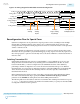
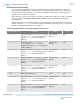
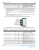
The following table shows the addresses and bits for switching between ATX PLL reference clock inputs.
The number of exposed pll_refclk ports varies according to the number of reference clocks you specify.
Use the ATX PLL reconfiguration interface for this operation.
Table 6-13: Register Map for Switching ATX PLL Reference Clock Inputs
Transceiver ATX PLL
Port
Description Address Bits
pll_refclk0
Represents logical refclk0. Lookup register
x113[7:0] stores the mapping from logical
refclk0 to the physical refclk.
0x113 (Lookup
Register)
[7:0]
pll_refclk1
Represents logical refclk1. Lookup register
x114[7:0] stores the mapping from logical
refclk1 to the physical refclk.
0x114 (Lookup
Register)
[7:0]
pll_refclk2
Represents logical refclk2. Lookup register
x115[7:0] stores the mapping from logical
refclk2 to the physical refclk.
0x115 (Lookup
Register)
[7:0]
pll_refclk3 Represents logical refclk3. Lookup register
x116[7:0] stores the mapping from logical
refclk3 to the physical refclk.
0x116 (Lookup
Register)
[7:0]
pll_refclk4 Represents logical refclk4. Lookup register
x117[7:0] stores the mapping from logical
refclk4 to the physical refclk.
0x117 (Lookup
Register)
[7:0]
N/A ATX refclk selection MUX. 0x112 [7:0]
When performing a reference clock switch, you must specify the lookup register address and respective
bits of the replacement clock. After determining the ATX PLL, follow this procedure to switch to the
selected reference clock:
1. Write 0x2 to address 0x0 of the PLL.
2. Read from the lookup register address and save the required 8-bit pattern. For example, switching to
logical refclk2 requires use of bits[7:0] at address 0x115.
3. Perform a read-modify-write to bits [7:0] at address 0x112 using the 8-bit value obtained from the
lookup register.
4. Write 0x3 to address 0x0 of the PLL.
UG-01143
2015.05.11
ATX Reference Clock Switching
6-21
Reconfiguration Interface and Dynamic Reconfiguration
Altera Corporation
Send Feedback