
User guide
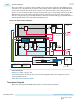
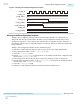

TX FIFO (Shared with Standard and Enhanced PCS)
The TX FIFO in each channel ensures a reliable transfer of data and status signals between the PCS
channel and the FPGA fabric. The TX FIFO compensates for the phase difference between the low speed
parallel PCS clock and the FPGA fabric clock. The RX and TX FIFOs are shared with standard and
enhanced PCS. In Hard IP mode, the TX FIFO works in register mode. In PIPE mode, the TX FIFO works
in low latency mode.
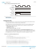
The TX FIFO operates in low latency mode in PIPE Gen1, Gen2, and Gen3 configurations. The Low
Latency mode incurs 3-4 cycles of latency when connecting with the FPGA Fabric. The FIFO empty and
the FIFO full threshold values are made closer so that the depth of the FIFO decreases, which decreases
the latency.
Related Information
Arria 10 Standard PCS Architecture on page 5-37
For more information about TX FIFO.
Gearbox
The PCIe 3.0 base specification specifies a block size of 130 bits, with the exception of the SKP Ordered
Sets, which can be of variable length. An implementation of a 130-bit data path takes significant resources,
so the PCIe Gen3 PCS data path is implemented as 32-bits wide. Because the TX PMA data width is fixed
to 32 bits, and the block size is 130 bits with variations, a gearbox is needed to convert 130 bits to 32 bits.
The gearbox block in the TX PCS converts the 130-bit data ( tx_parallel_data[127:0] +
pipe_tx_sync_hdr[1:0]) to 32-bit data required by the TX PMA as the datapath implementation is 32
bits to reduce usage of resources. The 130-bit data is received as follows in the 32-bit datapath: 34 (32 + 2-
bit sync header), 32, 32, 32. During the first cycle the gearbox converts the 34-bit input data to 32-bit data.
During the next 3 clock cycles the gearbox will merge bits from adjacent cycles to form the 32-bit data. In
order for the gearbox to work correctly, a gap must be provided in the data for every 16 shifts as each shift
is 2 bits for converting the initial 34-bit to 32-bit in the gearbox. After 16 shifts the gearbox will have an
extra 32-bit data that was transmitted out, and thus a gap is required in the input data stream. This gap is
achieved by driving pipe_tx_data_valid low for one cycle after every 16 blocks of input
data(tx_parallel_data).
Related Information
Gearbox on page 2-238
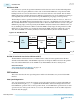
Receiver Datapath
This section describes the Block Synchronizer, Rate Match FIFO, and RX FIFO of the Gen3 PCS receiver.
Block Synchronizer
PMA parallelization occurs at arbitrary word boundaries. Consequently, the parallel data from the RX
PMA CDR must be realigned to meaningful character boundaries. The PCI-Express 3.0 base specification
outlines that the data is formed using 130-bit blocks, with the exception of SKP blocks.
The SKP Ordered Set can be 66, 98, 130, 162, or 194 bits long. The block synchronizer searches for the
Electrical Idle Exit Sequence Ordered Set (or the last number of fast training sequences (NFTS) Ordered
Set) or skip (SKP) Ordered Set to identify the correct boundary for the incoming stream and to achieve
the block alignment. The block is realigned to the new block boundary following the receipt of a SKP
Ordered Set, as it can be of variable length.
UG-01143
2015.05.11
TX FIFO (Shared with Standard and Enhanced PCS)
5-55
Arria 10 Transceiver PHY Architecture
Altera Corporation
Send Feedback