
User guide
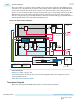
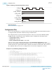

This section will focus on the basic blocks of PIPE 3.0-based Gen3 PCS architecture. The PIPE 3.0-based
Gen3 PCS uses a 128b/130b block encoding/decoding scheme, which is different from the 8B/10B scheme
used in Gen1 and Gen2. The 130-bit block contains a 2-bit sync header and a 128-bit data payload. For
this reason, Arria 10 devices include a separate Gen3 PCS that supports functionality at Gen3 speeds. This
PIPE interface supports the seamless switching of Data and Clock between the Gen1, Gen2, and Gen3
data rates, and provides support for PIPE 3.0 features. The PCIe Gen3 PCS will support the PIPE interface
with the Hard IP enabled, as well as with the Hard IP bypassed.
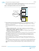
Figure 5-46: Gen3 PCS Block Diagram
32
32
32
32
Rate Match
FIFO
Auto-Speed Negotiation
Gen3 x1, x2, x4, x8
CDR
Control
TX
PMA
RX
PMA
PIPE Interface
TX PCIe Gen3 PCS
RX PCIe Gen3 PCS
TX Phase
Compensation
FIFO
RX Phase
Compensation
FIFO
Gearbox
/4
Standard
PCS
Block
Synchronizer
rx_clkout
pll_pcie_clk
tx_clkout
rx_coreclkin
rx_clkout or
tx_clkout
rx_clkout or
tx_clkout
FPGA
Fabric
tx_coreclkin
tx_clkout
Clock Divider
Parallel and Serial Clocks
Clock Generation Block (CGB)
Serial Clock
Input Reference Clock
ATX PLL
fPLL
tx_clkouttx_clkout
Serial Clock
Parallel and Serial Clocks
hclk for ASN Block
tx_clkout or rx_clkout
Related Information
PCI Express (PIPE) on page 2-228
For more information about PCIe Gen1, Gen2, and Gen3 implementation and configuration, refer to
"Supported PIPE Features."
Altera Hard IP for PCIe Users Guide
Transmitter Datapath
This section describes the TX FIFO and the Gearbox of the Gen3 PCS transmitter.
5-54
Transmitter Datapath
UG-01143
2015.05.11
Altera Corporation
Arria 10 Transceiver PHY Architecture
Send Feedback