
User guide
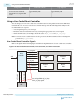
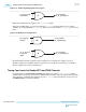
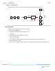

Figure 5-2: Serializer Block
The serializer block sends out the least significant bit (LSB) of the input data first.
Dn
D2
D1
D0
Parallel
Data
Serializer
DnD2D1D0
Parallel
Clock
Serial
Clock
Serial
Data
LSB
Transmitter Buffer
The transmitter buffer includes the following circuitry:
• High Speed Differential I/O
• Programmable differential output voltage (V
OD
)
• Main tap
• Programmable four-tap pre-emphasis circuitry
• Two pre-cursor taps
• Two post-cursor taps
• Power distribution network (PDN) induced inter-symbol interference (ISI) compensation
• Internal termination circuitry
• Receiver detect capability to support PCI Express and Quick Path Interconnect (QPI) configurations
5-2
Transmitter Buffer
UG-01143
2015.05.11
Altera Corporation
Arria 10 Transceiver PHY Architecture
Send Feedback