
User guide

Mix and Match Example
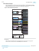
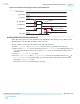
In the Arria 10 transceiver architecture, the separate Native PHY IP core and the PLL IP core scheme
allows great flexibility. It is easy to share PLLs and reconfigure data rates. The following design example
illustrates PLL sharing and both bonded and non-bonded clocking configurations.
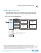
Figure 3-27: Mix and Match Design Example
Transceiver Bank
Transceiver Bank
ATX PLL
4 GHz
Transceiver Bank
ATX PLL, 5.15625 GHz
Transceiver Bank
ATX PLL
5.15625 GHz
Interlaken 12.5G
1.25G/9.8G/10.3125G
Interlaken 12.5G
Interlaken 12.5G
Interlaken 12.5G
Interlaken 12.5G
Interlaken 12.5G
Interlaken 12.5G
Interlaken 12.5G
Interlaken 12.5G
Interlaken 12.5G
10GBASE-KR
10GBASE-KR
10GBASE-KR
10GBASE-KR
1.25G/9.8G/10.3125G
1.25G/9.8G/10.3125G
1.25G/9.8G/10.3125G
PCIe Gen 1/2/3 x8
1.25G GbE
1.25G GbE
PCIe Gen 1/2/3 x8
PCIe Gen 1/2/3 x8
PCIe Gen 1/2/3 x8
PCIe Gen 1/2/3 x8
PCIe Gen 1/2/3 x8
PCIe Gen 1/2/3 x8
PCIe Gen 1/2/3 x8
Unused
Unused
Transceiver Bank
ATX PLL
6.25 GHz
MCGB
xN
x6
x1
xN
x6
MCGB
fPLL
2.5 GHz
mcgb_aux_clk0
ATX PLL, 4.9 GHz
fPLL, 625 MHz
x1
x1
x1
Interlaken12.5G
10GBASE-KR
1.25G/9.8G/10.3125G
Legend
1.25G GbE
PCIe Gen 1/2/3
Unused channel
PLL Instances
In this example, five ATX PLL instances and two fPLL instances are used. Choose an appropriate
reference clock for each PLL instance. The IP Catalog lists the available PLLs.
UG-01143
2015.05.11
Mix and Match Example
3-59
PLLs and Clock Networks
Altera Corporation
Send Feedback