
User guide
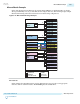


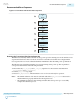

Figure 3-26: PLL Cascading
pll_refclk0 hssi_pll_cascade_clk
pll_powerdown pll_locked
pll_refclk0
pll_powerdown
fPLL or ATX PLL (Cascade Source) fPLL or ATX PLL (Transceiver PLL)
Steps to implement fPLL to ATX PLL cascading:
1. Instantiate the fPLL IP. Refer to Instantiating the fPLL IP Core on page 3-15 for detailed steps.
2. Set the following configuration settings for the fPLL IP core in the Parameter Editor:
• Set the fPLL Mode to Cascade Source.
• Set the Desired output clock frequency.
3. Instantiate the ATX PLL IP core (the second PLL in PLL cascading configuration). Refer to Instanti‐
ating the ATX PLL IP Core on page 3-5 for more details.
4. Configure the ATX PLL IP for the desired data rate and the reference clock frequency. Set reference
clock frequency for the ATX PLL same as the output frequency of the fPLL.
5. Connect the fPLL IP core (cascade source) to ATX PLL IP core (transceiver PLL) as shown in the
above figure. Ensure the following connections:
• The fPLL has an output port hssi_pll_cascade_clk. Connect this port to the ATX PLL's
pll_refclk0 port.
• For pll_powerdown, both the PLLs can share the same pll_powerdown or use independent power
down sources.
• Invert (perform logical NOT) pll_powerdown of the ATX PLL and then logical OR it (inverted
pll_powerdown) with the pll_lock signal of the first PLL. This ensures that the second PLL
(downstream PLL) is powered down until the first PLL has successfully locked to the input
reference clock. This prevents the second PLL from trying to lock until the output of the first PLL is
stable.
6. Ensure both the PLLs are calibrated. If the input reference clock is available at device power-up, no
special considerations are required to calibrate the PLLs. If the input reference clock is not available at
device power-up, then re-run the calibration for the first PLL. Only when the output of first PLL is
stable, re-run the calibration for the second PLL.
Notes:
• No special configuration is required for the Native PHY instance.
• The procedure for fPLL to fPLL cascading is similar to the one described for fPLL to ATX PLL
cascading.
• LC-fpll cascading mode is added to address the OTN and SDI jitter requirement. In this mode, LC-
PLL generates a relatively high and clean reference frequency in fractional mode. The reference is
driving the fPLL, which is running in integer mode. Overall cascaded two PLLs, synthesize a needed
frequency for a given data rate.
3-58
Implementing PLL Cascading
UG-01143
2015.05.11
Altera Corporation
PLLs and Clock Networks
Send Feedback