
User guide

Implementing x6/xN Bonding Mode
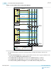
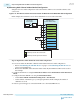
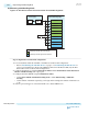
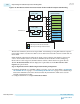
Figure 3-23: PHY IP Core and PLL IP Core Connection for x6/xN Bonding Mode
Transceiver PLL
Instance (5 GHz)
ATX PLL
Native PHY Instance
(10 CH x6/xN Bonding 10 Gbps)
TX Channel
TX Channel
TX Channel
TX Channel
TX Channel
TX Channel
TX Channel
TX Channel
TX Channel
TX Channel
Master
xN
x6
xN
xN
xN
x6
x6
x6
x6
x6
x6
Legend:
TX channels placed in the adjacent transceiver bank.
TX channels placed in the same transceiver bank.
CGB
x1
Steps to implement a x6/xN bonded configuration
1. You can instantiate either the ATX PLL or the fPLL for x6/xN bonded configuration.
• Refer to Instantiating the ATX PLL IP Core on page 3-5 or Instantiating the fPLL IP Core on
page 3-15 for detailed steps. Because the CMU PLL cannot drive the Master CGB, only the ATX
PLL or fPLL can be used for bonded configurations.
2. Configure the PLL IP core using the IP Parameter Editor. Enable Include Master Clock Generation
Block and Enable bonding clock output ports.
3. Configure the Native PHY IP using the IP Parameter Editor .
• Set the Native PHY IP TX Channel bonding mode to either PMA bonding or PMA/PCS
bonding .
• Set the number of channels required by your design. In this example, the number of channels is set
to 10.
4. Create a top level wrapper to connect the PLL IP core to Native PHY IP core.
3-54
Implementing x6/xN Bonding Mode
UG-01143
2015.05.11
Altera Corporation
PLLs and Clock Networks
Send Feedback