
User guide
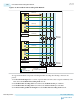
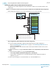
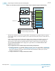

• In this case, the PLL IP core has mcgb_serial_clk output port. This represents the xN clock line.
• The Native PHY IP core has 10 (for this example) tx_serial_clk input ports. Each port
corresponds to the input of the local CGB of the transceiver channel.
• As shown in the figure above, connect the mcgb_serial_clk output port of the PLL IP core to the
10 tx_serial_clk input ports of the Native PHY IP core.
Figure 3-22: Multi-Channel x1/xN Non-Bonded Example
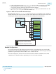
The ATX PLL IP core has a tx_serial_clk output port. This port can optionally be used to clock the six
channels within the same transceiver bank as the PLL. These channels are clocked by the x1 network. The
remaining four channels outside the transceiver bank are clocked by the xN clock network.
Transceiver PLL
Instance (5 GHz)
ATX PLL
Native PHY Instance
(10 CH Non-Bonded 10 Gbps)
TX Channel
TX Channel
TX Channel
TX Channel
TX Channel
TX Channel
TX Channel
TX Channel
TX Channel
TX Channel
CGB
x1
xN
Legend:
TX channels placed in the adjacent transceiver bank.
TX channels placed in the same transceiver bank.
Bonded Configurations
In a bonded configuration, both the high speed serial and low speed parallel clocks are routed from the
transmitter PLL to the transmitter channel. In this case, the local CGB in each channel is bypassed and the
parallel clocks generated by the master CGB are used to clock the network.
In bonded configurations, the transceiver clock skew between the channels is minimized. Use bonded
configurations for channel bonding to implement protocols such as PCIe and XAUI.
UG-01143
2015.05.11
Bonded Configurations
3-53
PLLs and Clock Networks
Altera Corporation
Send Feedback