
User guide
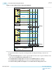
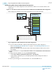
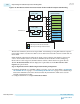

For PLL cascading, connections (1) and (3) are used to connect the output of one PLL to the reference
clock input of another PLL. Arria 10 transceivers support only fPLL to fPLL, fPLL to ATX PLL and ATX
PLL to fPLL cascading.
For PLL feedback compensation bonding, connections (2) and (4) are used to connect the master CGB's
parallel clock output to the PLL feedback clock input port.
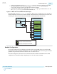
PLL feedback compensation bonding can be used instead of xN bonding. The primary difference between
PLL feedback compensation and xN bonding configurations, is for PLL feedback compensation, the
bonded interface is broken down into smaller groups of 6 bonded channels within a transceiver bank. A
PLL within each transceiver bank (ATX PLL or fPLL) is used as a transmit PLL. All the transmit PLLs
share the same input reference clock.
In xN bonding configurations, one PLL is used for each bonded group. In PLL feedback compensation
bonding, one PLL is used for each transceiver bank that the bonded group spans. There are no data rate
limitations in PLL feedback compensation bonding, other than the natural data rate limitations of the
transceiver channel and the PLL.
For feedback compensation bonding, the low-speed parallel clock must be the same frequency as the
reference clock for the PLL.
Note: Due to pending silicon characterization, Altera does not recommend using PLL cascading in ACDS
14.0 Arria 10 edition, 14.1 and 15.0 versions of the Quartus II software.
Related Information
Implementing PLL Cascading on page 3-57
Using PLLs and Clock Networks
In Arria 10 devices, PLLs are not integrated in the Native PHY IP core. You must instantiate the PLL IP
cores separately. Unlike in previous device families, PLL merging is no longer performed by the Quartus
II software. This gives you more control, transparency, and flexibility in the design process. You can
specify the channel configuration and PLL usage.
Related Information
Clock Networks
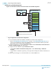
Non-bonded Configurations
In a non-bonded configuration, only the high speed serial clock is routed from the transmitter PLL to the
transmitter channel. The low speed parallel clock is generated by the local clock generation block (CGB)
present in the transceiver channel. For non-bonded configurations, because the channels are not related
to each other and the feedback path is local to the PLL, the skew between channels cannot be calculated.
Also, the skew introduced by the clock network is not compensated.
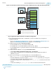
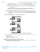
Implementing Single Channel x1 Non-Bonded Configuration
In x1 non-bonded configuration, the PLL source is local to the transceiver bank and the x1 clock network
is used to distribute the clock from the PLL to the transmitter channel.
For a single channel design, a PLL is used to provide the clock to a transceiver channel.
UG-01143
2015.05.11
Using PLLs and Clock Networks
3-49
PLLs and Clock Networks
Altera Corporation
Send Feedback