
User guide
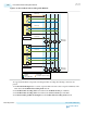
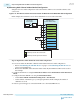
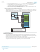
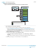
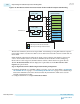

Figure 3-18: PLL Feedback and Cascading Clock Network
PLL Feedback and Cascading Clock Network
fPLL1
fbclk
refclk
C
ATX PLL 1
refclk
fbclk
M
Master CGB1
fPLL0
refclk
fbclk
C
ATX PLL 0
refclk
fbclk
M
Master CGB0
Bidirectional
Tristate Buffer
Bidirectional
Tristate Buffer
0 1 2 3
refclk Lines
fbclk Lines
C, M, and CGB Outputs
Legend
Transceiver Bank
PLL Cascading
PLL Feedback Compensation Bonding
Connection (1)
Connection (3)
Connection (2)
Connection (4)
To support PLL feedback compensation bonding and PLL cascading, the following connections are
present:
1. The divided clock output (the C counter output for fPLL or the M counter output for ATX PLL) of all
PLLs drives the feedback and cascading clock network.
2. The feedback and cascading clock network drives the feedback clock input of all PLLs.
3. The feedback and cascading clock network drives the reference clock input of all PLLs.
4. The master CGB’s parallel clock output drives the feedback and cascading clock network.
3-48
PLL Feedback and Cascading Clock Network
UG-01143
2015.05.11
Altera Corporation
PLLs and Clock Networks
Send Feedback