
User guide


PLL Feedback Compensation Bonding
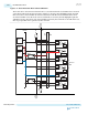
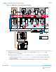
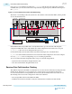
In PLL feedback compensation bonding, channels are divided into bonded groups based on physical
location with a three-channel or six-channel transceiver bank. All channels within the same six-channel
transceiver bank are assigned to the same bonded group.
In PLL feedback compensation bonding, each bonded group is driven by its own set of high-speed serial
and low-speed parallel clocks. Each bonded group has its own PLL and master CGB. To maintain the
same phase relationship, the PLL and master CGB for different groups share the same reference clocks.
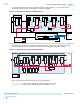
The steps below explain the PLL feedback compensation bonding process:
1. The same input reference clock drives the local PLL in each three-channel or six-channel transceiver
bank.
2. The local PLL for the bonding group drives the master CGB.
3. The master CGB feeds the x6 clock lines. The master CGB drives the transceiver channels in the
bonding group via the x6 clock network.
4. The parallel output of the master CGB is the feedback input to the PLL.
5. In this mode, all channels are phase aligned to the same input reference clock.
PLL Feedback Compensation Bonding Advantages over x6/xN Bonding Mode
• There is no data rate restriction. The x6 clock network used for PLL feedback compensation bonding
can run up to the maximum data rate of the device used.
• There is no channel span limitation. It is possible to bond the entire side of the device using PLL
feedback compensation.
PLL Feedback Compensation Bonding Disadvantages over x6/xN Bonding Mode
• It uses more resources compared to x6/xN bonding. One PLL and one master CGB are used per
transceiver bank. This causes higher power consumption compared to x6/xN bonding.
• The skew is higher compared to x6/xN bonding. The reference clock skew between each transceiver
bank is higher than the skew contributed by the xN clock network in x6/xN bonding.
• Because the feedback clock for the PLL comes from the master CGB and not from the PLL, the PLL
feedback compensation bonding mode has a reference clock limitation. The PLL's N-counter
(reference clock divider) is bypassed resulting in only one valid reference clock frequency for a given
data rate.
Note:
In order to minimize the reference clock skew for PLL feedback compensation bonding, use a
reference clock input near the center of the bonded group.
x6/xN Bonding Advantages over PLL Feedback Compensation Bonding
• x6/xN uses less resources compared to PLL feedback compensation bonding. Only one PLL and one
master CGB are required to drive all channels in the bonded group.
• x6/xN has lower skew compared to PLL feedback compensation bonding.
Related Information
Implementing PLL Feedback Compensation Bonding Mode on page 3-55
PMA and PCS Bonding
PMA and PCS bonding reduces skew between both the PMA and PCS outputs within a group of channels.
UG-01143
2015.05.11
PLL Feedback Compensation Bonding
3-45
PLLs and Clock Networks
Altera Corporation
Send Feedback