
User guide


You can clock the receiver datapath interface using one of the following methods:
• Quartus II selected receiver datapath interface clock
• User-selected receiver datapath interface clock
Channel Bonding
For Arria 10 devices, two types of bonding modes are available:
• PMA bonding
• PMA and PCS bonding
Note:
Channel bonding is not supported by GT channels.
PMA Bonding
PMA bonding reduces skew between PMA channels. In PMA bonding, only the PMA portion of the
transceiver datapath is skew compensated and the PCS is not skew compensated.
In Arria 10 devices, there are two PMA bonding schemes:
• x6/xN bonding
• PLL feedback compensation bonding
In either case, the channels in the bonded group need not be placed contiguously.
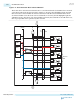
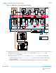
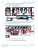
x6/xN Bonding
In x6/xN bonding mode, a single transmit PLL is used to drive multiple channels.
The steps below explain the x6/xN bonding process:
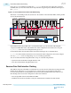
1. The ATX PLL or the fPLL generates a high speed serial clock.
2. The PLL drives the high speed serial clock to the master CGB via the x1 clock network.
3. The master CGB drives the high speed serial and the low speed parallel clock into the x6 clock
network.
4. The x6 clock network feeds the TX clock multiplexer for the transceiver channels within the same
transceiver bank. The local CGB in each transceiver channel is bypassed.
5. To drive the channels in adjacent transceiver banks, the x6 clock network drives the xN clock network.
The xN clock network feeds the TX clock mutiplexer for the transceiver channels in these adjacent
transceiver banks.
x6/xN Bonding Disadvantages
x6/xN Bonding has the following disadvantages:
• The maximum data rate is restricted based on the transceiver supply voltage.
• The maximum channel span is limited to two transceiver banks above and below the bank containing
the transmit PLL. Thus, the maximum span of 30 channels is supported.
Related Information
xN Clock Lines on page 3-33
3-44
Channel Bonding
UG-01143
2015.05.11
Altera Corporation
PLLs and Clock Networks
Send Feedback